Hey guys, what are the -6db response points for your amps? Mine is 2.6MHz right now. This is an easy test if you have a sine generator, just increase frequency until the response is half of it's ordinary value. (-6db=1/2)
I estimate my VAS miller compensation is about 56pF right now.
Kees, I think that in that amp the upper pair of outputs will be doing most of the work, with the lower pair acting more as a CCS than a push-pull pair. It would be easy to make current sharing more equal by using a bootstrap CCS with a 120R resistor, same as the GS resistor for the lower pair. If you want to tweak the current sharing this could be a trimmer.
If you don't want a bootstrap you could simply add a 120R Vgs resistor to the upper output pair, and increase the CCS current to adjust for the lost current. Then again, you could put a large cap in series with the 120R resistor and leave the CCS as is.
- keantoken
Hi
Have you some samples how to do this with a mosfet CCS, and what do you mean large cap with 120R in series, from source to gate mosfet?, I presume a mu follower looks like it.
I am a little stupid in mathematics, I make combinations, I have found bootstrapping ideas with bipolairs, and some depletion mosfets, not with enhanced ones.
thanks for your help.
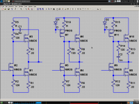
Here are some examples.
The first is the simplest. The compensation resistor, R4, is integrated into the bootstrap. Because the current through this resistor will mirror the current through R2, it's voltage drop will also be that of R2, to the Vgs of each output will be balanced and the outputs will equally share the load.
In the second, the CCS is still used, but it will have to have twice the VAS current because it must now also provide the current through R9.
In the third example, there is a cap in series with the 120R resistor, to block DC so the CCS current can be decreased. Overall, the first scheme should appeal for it's simplicity, and the second scheme should appeal to those who dislike caps. I don't know why anyone would use the third scheme, but it's an option.
Also, the .22R resistors you have placed on the drains of the upper outputs are not doing anything helpful. They should be placed at the sources instead, like in my schematic.
- keantoken
Attachments
Ahh thank you, yes now I recognized it.
it is impossible to get everything in my head, therefore I have a pc who do this for me haha.
I saw in my schematic that there was no load resistor of 8 ohm, therefore the simulations where good, now I have put it in and yes the amp got in stress, far more current from one side with half sinus as effect.
I go do experiments with save multisim, let you now the results..
Also, the .22R resistors you have placed on the drains of the upper outputs are not doing anything helpful. They should be placed at the sources instead, like in my schematic.
That is because of the elimination of the p mosfet, it was still the old way, I have not yet change that, but will do, peace by peace, oscillations with a common source is the reason I did it that way.
I am better in hybrides I think, but not to old to learn, thanks for sharing.
Last edited:
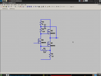
Kees, I also had the thought that really, the .22R source resistors are only needed on the lower outputs, since they set the bias current. But if we eliminate these resistors for the upper outputs, the current sharing is unbalanced again.
This is the solution I thought up. This way we can eliminate some redundant resistors and still have equal complimentary current sharing.
- keantoken
This is the solution I thought up. This way we can eliminate some redundant resistors and still have equal complimentary current sharing.
- keantoken
Attachments
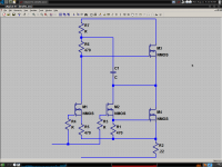
Unfortunately that won't work very well. Your VAS may appear like a differential but since the inputs are connected together they will only function in parallel. Let me suggest you try this version. Your version will have issues because it is not naturally balanced, and will waste a lot of energy through R16 to produce the voltage drive for the upper MOSFETs (measure dissipation of R16 and Q2).
Interesting idea to drive each output with it's own VAS. I wonder if it sounds better?
- keantoken
Interesting idea to drive each output with it's own VAS. I wonder if it sounds better?
- keantoken
Attachments
oohhh just 6.25 watt, good for wintertime.
But is nice for learning al this combinations of already invented wheels, I am lack of some mathematic things and names, I have never be on school for this, I learned as hobby at home.
The problem with fets is you can not switch like is with bjt, GS is very different as GD, only with depletion we can make wonders I think..
Last edited:
My circuit is not already adjusted for output bias. Output idle current will be determined by R7.
My idea in post 1904 is a dud...
Anyways this is not our thread, maybe we should go in private or make our own thread.
- keantoken
I agree, i have a thread pass labs basis idea here.
http://www.diyaudio.com/forums/pass-labs/155703-pass-labs-basis-allfet-amp.html
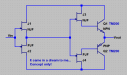
J1-2 seems functionally redundant to J3-4.
I'm not buying that proper bias will automagically just happen,
but I'll cut you some slack for being only a dream at this point.
You might look into Triodlington. Same exact thing, only completely different.
JFET is a triode, and senses 1/(Mu-1) portion of negative feedback from plate.
I suppose as a follower, would have slightly less than unity gain, but very linear...
Last edited:
The Eagle has Landed!!
Folks,
We are almost good to go for the FetZilla Group Buy. I have all the semis, the pcbs have arrived sooner than I expected, and I will commence soldering all the VAS devices onto the pcbs this weekend.
The pcbs are just GREAT!!
Accordingly, can all those who have not yet contacted me
SEND DETAILS OF FULL NAME, ORDER QUANTITY, SHIPPING ADDRESS, AND PLEASE PAY ME ASAP THROUGH PAYPAL IN AUSSIE DOLLARS ($AUD60 including parts, $AUD50 just boards).
MY EMAIL IS ASPEN01 -at- OPTUSNET.COM.AU (Same email for Paypal)
Happy days, I'm pleased this has resolved, it was a long, long wait!
Cheers,
Hugh
Attachments
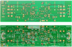
Earlier this week I was looking through an old IR HexFET data book and read AN-948. That looked like just the sort of FET amp that I wanted to build for a project I have in mind. Specs were good, parts count small. Then I got on the web and searched around to see if anybody had already built one of these, maybe improved it. After a couple of search tries, Google found this thread. It has taken two days of my (so-called) spare time to read this thread. All of the contributors here should be congratulated, it is great to find a web discussion with a high signal-to-noise ratio, and with such successful outcome, that remains true to the original post intent. Now I am off to email Hugh, I need to buy some pcbs.
Update
Nice boards Hugh, I think the're gonna make a lot of people very happy.
My amps are progressing nicely also. Here is a summary of my findings:
1) Choke Supplies in themselves, if designed correctly, do not sound slow or sluggish but because they can reduce PSU noise so drastically the amp can be, infact, has to be, adjusted to "match" the transparency that the supplies allow.
2) It would seem that an amp like mine that has lower CLG ( x11 ), and thus more FB and therefore requires a small amount of compensation, can still sound very lively & engaging so long as the compensation is kept to a minimum.
3) I'm amazed that without changing the actual "spec" the sound of the amp can be changed very much. At present I have my amps in fast and exciting mode and I can see why Greg & Naim fans around the world are so enthusiastic about it. It just sounds like the musicians, and the amp, are really enjoying making music.
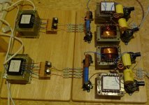
After one more mod on my hand made prototype boards I will then build an exact copy using my PCBs, put the supplies & amps into boxes, and then continue my investigations in the living room.
I attach a pic of my breadboarded choke supplies for your amusement")
Nice boards Hugh, I think the're gonna make a lot of people very happy.
My amps are progressing nicely also. Here is a summary of my findings:
1) Choke Supplies in themselves, if designed correctly, do not sound slow or sluggish but because they can reduce PSU noise so drastically the amp can be, infact, has to be, adjusted to "match" the transparency that the supplies allow.
2) It would seem that an amp like mine that has lower CLG ( x11 ), and thus more FB and therefore requires a small amount of compensation, can still sound very lively & engaging so long as the compensation is kept to a minimum.
3) I'm amazed that without changing the actual "spec" the sound of the amp can be changed very much. At present I have my amps in fast and exciting mode and I can see why Greg & Naim fans around the world are so enthusiastic about it. It just sounds like the musicians, and the amp, are really enjoying making music.
After one more mod on my hand made prototype boards I will then build an exact copy using my PCBs, put the supplies & amps into boxes, and then continue my investigations in the living room.
I attach a pic of my breadboarded choke supplies for your amusement
Attachments
Last edited:
- Status
- This old topic is closed. If you want to reopen this topic, contact a moderator using the "Report Post" button.
- Home
- Amplifiers
- Solid State
- JFET input, MOSFET VAS, LATERAL output = Perfect!!