These are the output fets I'll use, unless you can suggest a better alternative:
http://www.profusionplc.com/pro/gex/prodGen.html?prdtyp=lateral mosfet
Which model do you think is the best, maybe the ECW20N20-Z and it's complement:
http://www.profusionplc.com/pro/gex/pcatdtl0?ipartno=ECW20N20-Z
http://www.profusionplc.com/pro/gex/prodGen.html?prdtyp=lateral mosfet
Which model do you think is the best, maybe the ECW20N20-Z and it's complement:
http://www.profusionplc.com/pro/gex/pcatdtl0?ipartno=ECW20N20-Z
Last edited:
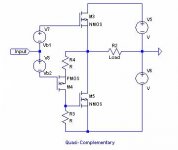
This is the most perfect amplifier I have spiced.
It is simple but yet very, very good.
- JFET input with minimal offset problems.
- MOSFET VAS for speed and gain
- LATERAL output for be a light load to VAS
When CLass AB operation, 350mA bias, it shows only
THD 0.00018% at 1 Watt
And there is almost no increase of THD at 25 Watt output
Enjoy!!")
lineup,what simulator do you use?
this here is my take on a higher power version...
I included a cascode and a current mirror...the latter to get better control over the DC drift
The output stage is kind of special as the negative tempco of the laterals keeps the BTJ's from running away...and while the BTJ's are supplying all the current..the Laterals never leave Class A or go so low in current that the bipolars switch off..(they go down to app 20mA when the amplifier is driven with 2 V)
Attachments
Did you download MultiSim 11?
As recommended by me in another topic.
could you PM me on this, I have question ( I couldn't seem to PM you )
thx
MiiB,
Nice work. Of course, this is now a very different amplifier; multiple rails, three output pairs, but I like the use of lateral FET drivers with bipolar outputs. The cascode permits use of low voltage jfets, improving reliability by lowering dissipation. Clever.
I can see why you are using a current mirror, on the face of it is is elegant. However, the source resistor for M3, the reference arm of the current mirror, is non-linear because of the BE junction of Q3. I would be inclined to use Q3 and Q14 as standalone CCSs, without the mirror, and simply use 10R degeneration in the source to rail. The 320mA quiescent current of the lateral FET drivers is VERY high, however, this is a serious dissipation with 60V rails (19 watts per device!!). Nevertheless, I cannot argue with the results; the profile of the distortion looks very good, very like Class A, with predominance of musical H2 and H3 and very little else.
However, to verify hunches someone must build it. There are a hundred simmed circuits around here, but few are built and further commented on. Things like offset control, bias stability with temperature, Bode stability and sonic presentation are complete unknowns until we have a real amp on the ground, so I would encourage someone to build it, a la Ostripper and Carlos, who have the greatest build profiles of anyone here.
Cheers,
Hugh
Last edited:
Member
Joined 2009
Paid Member
this is handy - I'm looking for some Lateral's as an option for my tube-SS hybrid project. I'll be interested to hear how you like these.
Last edited:
Hugh...
In my sims the laterals are running at app 200 mA and dissipating app 15W the following BTJ's are dissipating app 7 W... all is easy to adjust simply by altering the bias spread resistor...
I may have gone a little overboard in setting the casode voltage by using a CCS for that... purpose alone...
The VAS Fet runs on 17 mA set by the LED based CCS in the buttom...
I would like to separate the two stages a little more... could be done by inserting a CCS in the top of the Jfet..??
Hi Michael,
It's clearly a very good circuit, as there is some distortion cancellation going on, according to the sim that is. I would not expect levels of distortion this low from a more conventional topology, so my comments are entirely advisory and may not actually improve things. I suspect that your VAS source circuit is cancelling some of the expected distortion, since my sims do not come anywhere close.
However, there may be some error in the simulation. If we assume the quiescent current through each output is somewhere around 110mA, then drop across the emitter resistors is only 11mV and across the BE of out output typically 620mV according to my experience. This gives a combined 2x620 + 2x11 or 1.362V between the bases of the outputs, and hence the sources of the two drivers. With 4.4R between them, this gives about 310mA, so your simulator result of 200mA looks very low to me. Something is wrong there....
Can I suggest a few things to try?
How about replacing R7 and R8 with a single resistor of 12R, giving us a driver current of around 116mA apiece. This is a nice high figure and limits dissipation to 6.85W. Further, the laterals will never turn off, and the minority carriers in the bases of the outputs can be swept away with a large size cap across this single resistor, around 470nF should do it, metallised PP.
I think each output should have a 2R2 stopper on each base to remove any threat of local oscillation.
You can set a cascode voltage on the input jfet very simply with a zener of say 15V and a good sized cap. Much less componentry, and just as quiet. Another option is a TL431 which is also very effective and simple.
Michael, could you please send the .asc with tail changed to lts to my email address via my website? I'm curious to know why this amp has such low distortion, I think it's impressive.
Thank you for sharing such a good circuit with us!
Hugh
I'll surely send the circuit...
I have attached the Laterals to the output after the philosophy that the laterals take care of the refinements and the let the BJT's do the crude work.
By doing it this way the turnoff of the BTJ's is also very soft and gradual..As set up here you need 2.5 V to bring it to the rail...
I must admit that your right about the 4.4 resistors they were changed to lover values when simming the circuit...2.7 ohm..hence my lower currents Sorry
BTW.. I have seen that the firmer you clamp things the better the performance is...like if you have a reference based on resistors..it not very firm, and you get some increase in higher order distortion.. compared to the firmer lock down made by LED's as per example
6.85W. Further, the laterals will never turn off, and the minority carriers in the bases of the outputs can be swept away with a large size cap across this single resistor, around 470nF should do it, metallised PP.
Hugh,
Would you mind explaining this concept in a little more detail? I'm eager to learn more about the purpose of the capacitor.
Many thanks!
Greg.
SWF,
Charge suckout circuits are explained by Self in his EFII configuration. It means simply running a single resistor from one driver source to the other, with a cap across it. This acts to absorb minority carriers from the active output device as it turns off by charging the capacitor as the other side turns on. It's a well known trick and works nicely.
I have done some extreme simplification on this excellent design, and changed it to a deep Class AB power amplifier, running around 175mA in the output stage devices. It still dissipates just less than 70 watts at idle, but it's manageable - as a Class A running 1.2A it dissipated over 430W, so it's carbon emissions are just a little lower.
Performance is essentially unchanged, around 0.00095% at +20dBU (13W into 8R @ 1KHz) which is close enough for government work.
The weak point is the extreme tetchiness of output offset control. It depends hugely on the pinpoint accuracy of the current source which supplies Q1, the JFET. This would be best solved with a servo, I suspect.
Thanks to Michael for an excellent design.
Cheers,
Hugh
Last edited:
does that mean that I1 must temperature compensate for Q1, exactly?The weak point is the extreme tetchiness of output offset control. It depends hugely on the pinpoint accuracy of the current source which supplies Q1, the JFET. This would be best solved with a servo, I suspect.
Would a carefully matched pair of jFETs, thermally coupled together, be in the ballpark?
Hi Andrew,
Yes, pretty much. I have not yet considered this in depth, merely noted it, but I suspect that nothing short of a servo would resolve the issue completely.
This frustrates me somewhat, as I try to avoid servos - added complexity and all that jazz.
The extreme sensitivity, the direct result of a magnified offset due to the DC coupled fb divider network, is too great to compensate with a matched jfet. In truth, to match two jfets within a couple of percent would need a sample of more than twenty anyways..... best to dynamically null the offset with a servo.
Hugh
Last edited:
Yes an add-on servo could be used.too great to compensate with a matched jfet. In truth, to match two jfets within a couple of percent would need a sample of more than twenty anyways.....
I have been selling 1% and 0.5% matched pairs for a few years now.
That is not Idss selected to 1% or 0.5%.
That is Id matched with a common voltage fed to Vgs, to that accuracy over the range from 100% Idss down to ~25% Idss.
Buying software
I did not know that Torrent licenses software. Exactly how does that work ?
MultiSim 11 torrent <- search google
We are quite many now using MultiSim
Welcome to diyAudio, samolet
I did not know that Torrent licenses software. Exactly how does that work ?
- Status
- This old topic is closed. If you want to reopen this topic, contact a moderator using the "Report Post" button.
- Home
- Amplifiers
- Solid State
- JFET input, MOSFET VAS, LATERAL output = Perfect!!