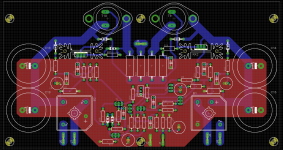
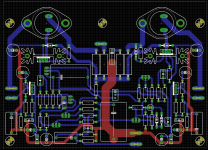
NAP140/NCC200 clone with onboard PSU.
Clone of NCC200, but without output inductor.
Schematic doesnt contain the correct values yet and not all the caps/transistors are the right ones. But I wanted to get most of the layout done first to get a feel of the size of it.
Size is about 22 x 12 CM.
Clone of NCC200, but without output inductor.
Schematic doesnt contain the correct values yet and not all the caps/transistors are the right ones. But I wanted to get most of the layout done first to get a feel of the size of it.
Size is about 22 x 12 CM.
Attachments
I'm not sure I would want to put the bridge rectifiers on the amp pcb
Thought about that as well, they might make too much noise.
Maybe Ill leave them off in a new version. Could fit 1 PSU cap more pr rail
instead of the rectifier.
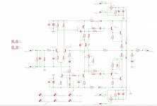
Schematic doesnt contain the correct values yet and not all the caps/transistors are the right ones.
Hi Neutrality,
I have been caught using generic transistors before. Be careful of the pin-outs of the first 2 stage transistors as optimum PCB design can depend on the pin order, especially when the transistor is connected to a heat-sink. Sometimes you can just rotate them 180 degrees without a problem.
Did you miss the input cap on purpose?
regards
Generic transistors are just used to get the layout going, I will be going over each of them to check for correct pin out/package and change those who needs to be changed. The same goes for the caps, the ones currently used are just placeholders.
Wrt the input cap, ehm, thats a mistake on my part. I forgot it.

Last edited:
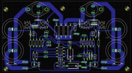
Removed onboard rectifiers, added correct caps, and redid the whole board more or less as the real NCC200 board, but with onboard caps and more space between the output transistors. GND plane has been removed as well. Only thing missing is correct version of 3 of the transistors.
And it is now a single sided board, easier and faster for me to make a prototype this way. Before I spend any real money on a professionally made PCB.
Output transistors will be either MJ15003, BUV20 or BUX20 from Semelab(50A, 350W max dissipation)
And it is now a single sided board, easier and faster for me to make a prototype this way. Before I spend any real money on a professionally made PCB.
Output transistors will be either MJ15003, BUV20 or BUX20 from Semelab(50A, 350W max dissipation)
Attachments
Last edited:
That was something I have been considering. Theres plenty of room for it.
There should be enough room for it to be a drop in replacement.
But if not, I can move most of the bottom circuit more to the left if needed. One of the reasons why I didnt make it as compact as I could, always good to have more space for changing components.
Currently looking at different versions of the basic circuit, including modifications from SKA Audio. But they might change the circuit to something else, but lets see about that.
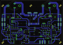
Well, after trawling through the web for NAP140 info and general info about mods to Naim amplifers I came across
For want of a better name: the HackerNAP board - Page 57 - pink fish media
and
Modifying Naim Audio power amplifiers
So now its a HackerNap by CBA. But with TO-3 transistors.
Redoing the layout didnt take too long.
Now I just need some spare time so I can build a proto board.
For want of a better name: the HackerNAP board - Page 57 - pink fish media
and
Modifying Naim Audio power amplifiers
So now its a HackerNap by CBA.
But with TO-3 transistors.Redoing the layout didnt take too long.
Now I just need some spare time so I can build a proto board.
Attachments
Hi there,
I'm the guy that put together the original HackerNAP/HackerCAP project. It's based on the Naim NAP and Avondale NCC200 circuits, with some Acoustica modifications and other bits n bobs gleaned from the Internet. I don't claim any credit for designing those circuits or components, only for amalgamating them in one place for one design.
I did, however, layout the HackerNAP (and the corresponding power supply, the HackerCAP) PCBs very painstakingly. One of the design goals was to think very carefully about separating the power supplies for the front-end and for the output stage. Among those considerations was the arrangement and design of the 0V configuration, which is not very straightforward. The separate power supplies are also highly customised to account for the different needs of the output stage and the front end.
The design that you've come up with is, at best, compromised compared to the original, and I'm afraid your schematic/PCB has at least one error: you have placed R23 (a 15R) directly in series with the amp output. This will not work without the corresponding output inductor! The 15R is supposed to be in parallel with the output inductor and is merely there to stop ringing. Without the inductor, you're going to (at best) ruin the sound of the amp. In all likelihood you'll quickly release the Magic Smoke.
The layout of your board also negates many (most!) of the benefits that the amp & PSU design were designed to bring to the table, especially the grounding/PSU layout, which is the amp's major design feature and was designed to alleviate some of the problems associated with the NAP/NCC designs. For example, the shared 0V returns on your board are going to do you no favours (eg. the Zobel is connected directly to the signal 0V; the signal 0V is also slung right between the power 0Vs, which will modulate the signal; the front-end and output stage 0Vs share a common PCB track, etc etc etc ), and honestly there are so many compromises with your board layout that if you haven't already made it, I suggest you stop right now and do some redesign work.
To help you along, please take a look at the build manual and schematic for the original HackerNAP. It's available for free here: HackerNAP project page. I urge you to read that page carefully before proceeding. In fact, don't just read the web page - download the actual build manual because it contains much more information, photos, diagrams, close-ups, etc etc.
You'll also find the PCB Gerber files, bill of materials, and schematic freely downloadable. This is an open-source project and you are of course welcome to do with it as you wish; I would, however, urge you to reconsider the design that you are embarking on because it is a big step backwards over the original. If you do go ahead with this design I would be grateful if you called it something other than a HackerNAP
Having said all of that, please feel free to ask any questions. I'll do my best to answer, and hopefully we can come up with something that allows you to use TO3 devices without compromising the HackerNAP design. Hell, I might even add another variant of the PCB to incorporate TO3 devices if there's any interest from other folks.
Cheers,
Carl
....
Those points have been adressed a few days ago, just havent gotten around to post it here.
As you probably know most PCB layout design work is usually a WIP, with continous tweaking taking place. From first draft to the final version a lot of stuff can and do happen.
The 2 x FE gnd, 2 x OP gnd, zobel gnd and signal gnd are all seperated.
Regarding R23, there will be a inductor, just havent put it on the schematic.
Attachments
Last edited:
Just want to report a couple of things
It has been my experience that you don't need the inductor on the output.
However this amplifier is prone to oscillation. What ever you do don't use drivers such as 2sc4793 or 2sc5171, these devices guarantee oscillation.
I was able to stop the oscillation by putting a small cap across collector and base (eg 47pF) of the offending driver. However in the end I decided to revert back to TIP devices.
I didn't do listening tests, so can't say wether it is better to use the fastest drivers available and then erradicate the oscillation by the use of the appropriate cap or whether it is better to use devices that don't cause oscillation in the first place.
Just something to keep in mind.
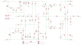
I was wondering if anyone here could explain the choice of the values of Capacitors and Resistors in the small network that feeds the base of TR7 and TR8. I am certain that these should be different values according to the choice of transistors and the layout of the circuit. Perhaps we are just slavishly copying this from the original Naim Circuit without really understanding it??
John
John
For anyone who's interested, I tweaked the original design and added TO3 output devices. Gerber files are available here: HackerNAP TO3 Gerbers.
I would still encourage you to go for the original version over this one. There are a few good reasons, mainly: the output transistor decoupling caps are (by virtue of the physical footprint of the TO3 transistors) quite far from the transistors they're supposed to be decoupling. There's at least an inch of PCB track between the caps and the trannies, which is far from ideal.
The new layout also puts the output trannies quite some distance from the drivers, which is also not ideal. It also makes the PCB size larger. You may or may not care Anyway, the new version is there for you to use if you like.
@Neutrality: What it is the goal of your design? If you've got ideas for improvements to the HackerNAP/CAP I'm interested in hearing them. Perhaps they can be incorporated into the next revision so that we all benefit - like I said, this is an open source design and anyone is welcome to contribute.
I do understand, however, if you would like me to butt out of your thread instead of hijacking it with criticisms of your design!
@John: You're spot on when you say the values are slavishly copied from the original circuits (some values are NCC, some NAP). The aim of the HackerNAP was to concentrate on improving the power supply and grounding layout... basically pimping the existing amp instead of doing a redesign of it! I'm always happy to listen to new ideas, though!
Carl
I would still encourage you to go for the original version over this one. There are a few good reasons, mainly: the output transistor decoupling caps are (by virtue of the physical footprint of the TO3 transistors) quite far from the transistors they're supposed to be decoupling. There's at least an inch of PCB track between the caps and the trannies, which is far from ideal.
The new layout also puts the output trannies quite some distance from the drivers, which is also not ideal. It also makes the PCB size larger. You may or may not care
Anyway, the new version is there for you to use if you like. @Neutrality: What it is the goal of your design? If you've got ideas for improvements to the HackerNAP/CAP I'm interested in hearing them. Perhaps they can be incorporated into the next revision so that we all benefit - like I said, this is an open source design and anyone is welcome to contribute.
I do understand, however, if you would like me to butt out of your thread instead of hijacking it with criticisms of your design!
@John: You're spot on when you say the values are slavishly copied from the original circuits (some values are NCC, some NAP). The aim of the HackerNAP was to concentrate on improving the power supply and grounding layout... basically pimping the existing amp instead of doing a redesign of it! I'm always happy to listen to new ideas, though!
Carl

@Neutrality: What it is the goal of your design? If you've got ideas for improvements to the HackerNAP/CAP I'm interested in hearing them. Perhaps they can be incorporated into the next revision so that we all benefit - like I said, this is an open source design and anyone is welcome to contribute.
Well, firstly, I like doing PCB layouts, weird, I know.
Secondly, planning on making an amplifier, but not sure which yet. But I want to make my own PCB,s not just for fun but to learn.
Made PCB layouts for First Watt F5, with triple outpust and cascoded input, HackerNap but with TO-3 transistors, and lastly ESP P3A with TO-3 output transistors and a few other changes.
Last edited:
Well, firstly, I like doing PCB layouts, weird, I know.
Secondly, planning on making an amplifier, but not sure which yet. But I want to make my own PCB,s not just for fun but to learn.
Made PCB layouts for First Watt F5, with triple outpust and cascoded input, HackerNap but with TO-3 transistors, and lastly ESP P3A with TO-3 output transistors and a few other changes.
Very cool. The only part I disagree with is that you haven't made a layout for a HackerNAP unless you maintain the star-grounding and power supply separation ;-) Until then it's "only" a NAP/NCC clone!
Very cool. The only part I disagree with is that you haven't made a layout for a HackerNAP unless you maintain the star-grounding and power supply separation ;-) Until then it's "only" a NAP/NCC clone!
Well, you might have a point. The schematic used is definately HackerNap, but the layout is my own.
- Home
- Amplifiers
- Solid State
- NAP140/NCC200 Clone with PSU