If there have been no mistakes the circuit is correct.
I have only a basic grasp of electronics, I've not studied it for years, and I'm seeking a basic understanding of how feedback works in this vintage circuit.
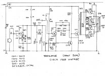
My focus is 15VT2 and 3 and 5VT1.
Ideally, quiescent currents and bias voltages ought to remain static. In a dynamic situation, set bias voltages/currents ought to remain static.What steps have been taken in this circuit to try to maintain steady bias voltages?
Then we have the issue if reducing distortion. What steps if any have been taken in this circuit around the devices mentioned to reduce distortion of the signal by way of negative feedback?
15VT2 can take a signal (from a circuit that produced an alarm sound). But, can 15VT2 been seen solely as a feedback element in it's own right? (Is it the case that 15VT2 can take an input - just a nice bonus?)
I hope my questions make sense.
I don't think 15VT2 really amplifies.
Thanks.
I have only a basic grasp of electronics, I've not studied it for years, and I'm seeking a basic understanding of how feedback works in this vintage circuit.
My focus is 15VT2 and 3 and 5VT1.
Ideally, quiescent currents and bias voltages ought to remain static. In a dynamic situation, set bias voltages/currents ought to remain static.What steps have been taken in this circuit to try to maintain steady bias voltages?
Then we have the issue if reducing distortion. What steps if any have been taken in this circuit around the devices mentioned to reduce distortion of the signal by way of negative feedback?
15VT2 can take a signal (from a circuit that produced an alarm sound). But, can 15VT2 been seen solely as a feedback element in it's own right? (Is it the case that 15VT2 can take an input - just a nice bonus?)
I hope my questions make sense.
I don't think 15VT2 really amplifies.
Thanks.
An externally hosted image should be here but it was not working when we last tested it.
Attachments
Last edited:
An externally hosted image should be here but it was not working when we last tested it.
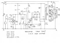
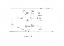
If there have been no mistakes the circuit is correct.
There was in fact a mistake. 15VT2 emitter and collector needs reversing as shown. So correct circuit is shown here.
Attachments
Last edited:
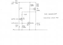
Here is the core circuit under consideration. Stripped down the dc essentials.
Does it ring any bells? Make any sense? How might it work? Can it work? Thanks.
The arrangement controls the current in VT1 by servoing the current in the 3.3R resistor.
Vt2 maintains a DC voltage equal to Vbe+ VE*12/(12+220) across the resistor (plus a small supplement due to the 132R).
Dynamically, the 132R determines the transconductance on input 2: G2= 132/(Rin*3.3).
The transconductance from in1 is practically direct: G1~=1/3.3
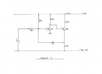
Is circuit 2 pretty much the same as circuit 1?
If so, the core of my circuit is something like Shunt Series FB Pair Amplifier as per at page 5:http://www-personal.engin.umd.umich.edu/~fmeral/ELECTRONICS%20II/05%25c3-Discrete%20BJT/DiscreteAmplifierProject.pdf
R26 is supposed to be equivalent to RX. 132R and VT2 is instead of RF.
If so, the core of my circuit is something like Shunt Series FB Pair Amplifier as per at page 5:http://www-personal.engin.umd.umich.edu/~fmeral/ELECTRONICS%20II/05%25c3-Discrete%20BJT/DiscreteAmplifierProject.pdf
R26 is supposed to be equivalent to RX. 132R and VT2 is instead of RF.
Attachments
Last edited:
Except VT2 is in the path, and introduces some level-shiftingIs circuit 2 pretty much the same as circuit 1?
.
More or less, but there is little point trying that hard to put a name on something.If so, the core of my circuit is something like Shunt Series FB Pair Amplifier as per at page 5:http://www-personal.engin.umd.umich.edu/~fmeral/ELECTRONICS%20II/05%25c3-Discrete%20BJT/DiscreteAmplifierProject.pdf
R26 is supposed to be equivalent to RX. 132R and VT2 is instead of RF
The circuit is simple enough to be analyzed on its own, without a reference to a known topology.
Okay, I now see that my original circuit is essentially a BJT shunt series feedback amplifier or shunt series pair.
What I'm trying to do is to remove VT2 and be left with VT1 and VT3, a shunt series pair.
There are some references on the internet that might enable me to go though the design of the shunt series pair. I'd like to see what Horowitz said on page 872, but I have no access to this.
Anyway, I've decided to try my hand at designing a shunt series pair. I know little about electronic design, but will give it a shot. Will teach me some electronics.
- Status
- This old topic is closed. If you want to reopen this topic, contact a moderator using the "Report Post" button.
- Home
- Amplifiers
- Solid State
- Feedback arrangement in vintage 50W amplifier