What do you mean by sensitive? Say if I set for 10mA, how much would I expect to change? Seems like if too much imbalance in current, the 47K resistor can be reduced to lessen the effect. Say even down to 10K, it's still higher than if you resort to resistor load of the IPS.
Exactly.
Cheers,
Bob
Well I hope it works; I'll find out soon enough, my boards will arrive any day now.
Sorry to ask question on Mr. Cordell's thread.
But your schematic and the transistors you picked is very similar to my design. I have a few questions:
1) I use KSA992 and KSC1845 for all the front end transistors. You use BC550 and BC560. Any particular reason? I did look into this also, but I ended up using one pair for all the small signal transistors because I like the low Cob that implies lower capacitance on the others.
2) what is the advantage of using Q21 and Q22 combined for the Vbe multiplier? I use KSC1845 alone and mount it onto the heat sink.
3) I use 3EF for OPS, but I use all NPN and PNP on one side to keep it simple.
I just want to hear your thinking.
Thanks
Thank you very much Mr. Cordell. I designed for 10mA through the VAS, It does not matter whether it is 15mA or 5mA(+/-5mA). I think I have it covered. I used KSA1381 and KSC3503 with 50V max rail. I think I can take the variation.
Just for curiosity, I use 300ohm for emitter degeneration for all 4 of the transistors of both differential pair. Does that help a lot on the balance? I run 2mA tail current for each LTP.
Thanks
I believe that the current mirrors should always be degenerated with emitter resistors. I generally go for about 10:1 degeneration, meaning that RE is about 10X re of the transistor. A transistor running 1mA would thus have an RE of about 260 ohms.
The amount of degeneration in the current mirror also affects the noise contribution of the current mirror, with smaller RE causing a higher noise contribution.
Finally, in the complementary arrangement with the current mirror shunt resistors, note that the choice of the value of the current mirror emitter resistors is inter-twined with the choice of the tail current and amount of degeneration in the VAS emitter circuit.
Cheers,
Bob
I gave it some thoughts, seems like the degeneration of both the differential transistors and the transistors in the current mirror is the KEY for matching. Notice I use 1K to degenerate the current mirror transistors. This will drop 1V across the resistor. This will more than swamp out the Vbe difference. I use 300ohm degeneration for the differential transistor, that's 300mV.I think I saw VAS current change of 2-3 mA, and that was by Hfe mismatching at one pair of transistor alone, before any Vbe mismatching and temperature stepping simulation that I didn't bother trying.
Yes, you can reduce the load resistor but that would further negates the point of using a current mirror.
I don't know why you think it's so important about hfe matching as any imbalance in current will be compensated by the action of the degeneration resistors. There is no other way around it. It's like when one transistor tries to pull more current, the voltage drop over the emitter resistor literally FORCE the other transistor to conduct more to fight for the constant current!!!!
To me, the difference in Vbe between the two transistors of the differential pair and the current mirror is even more important than the hfe if you have plenty of degeneration. That's the reason I sacrifice 1V of headroom and use 1K on the current mirror, sacrificing gain of the IPS and use high value degeneration resistor to overcome the matching problem.
These are all common sense theory, not relying on simulation. You design to force the circuit to match. Then I use 2EF on the VAS to up the input impedance to get back the gain at LF. Then make the VAS a current integrator at HF as Mr. Cordell described so nicely.
Last edited:
Sorry to ask question on Mr. Cordell's thread.
But your schematic and the transistors you picked is very similar to my design. I have a few questions:
1) I use KSA992 and KSC1845 for all the front end transistors. You use BC550 and BC560. Any particular reason? I did look into this also, but I ended up using one pair for all the small signal transistors because I like the low Cob that implies lower capacitance on the others.
2) what is the advantage of using Q21 and Q22 combined for the Vbe multiplier? I use KSC1845 alone and mount it onto the heat sink.
3) I use 3EF for OPS, but I use all NPN and PNP on one side to keep it simple.
I just want to hear your thinking.
Thanks
Hi Alan
I'm keen to see your circuit.
I chose the high gain, low noise BC5x0 transistors for the complementary LTPs because I believe these parameters make them ideally suited for this application. High Vce transistors such as the KSA992/KSC1845 tend to be compromise these important parameters to achieve higher breakdown voltages.
I could have used the BC5x0 in the LTP cascade positions also, since the rail voltage specified are within their limits; however, I wanted to be able to scale the design at a future point with minimal changes.
Q21 and Q22 make up the CFP bias spreader; the high gain is useful with symmetrical voltage gain stages where the bias voltage is indeterminate. Q21 is a TO-126 package fixed to one of the output transistors, the other is a free-standing TO-92.
The benefit of this particular EF3 topology is that the driver and pre-driver temp co's cancel, simplifying thermal compensation. The other benefit is that the pre-drivers are bootstrapped to the output and pass only the bias voltage; high gain small signal transistors can be used where other topologies would call for parts with higher breakdown voltages and lower gain.
All this is covered in Bob's wonderful book.
Last edited:
I gave it some thoughts, seems like the degeneration of both the differential transistors and the transistors in the current mirror is the KEY for matching. Notice I use 1K to degenerate the current mirror transistors. This will drop 1V across the resistor. This will more than swamp out the Vbe difference. I use 300ohm degeneration for the differential transistor, that's 300mV.
I don't know why you think it's so important about hfe matching as any imbalance in current will be compensated by the action of the degeneration resistors. There is no other way around it. It's like when one transistor tries to pull more current, the voltage drop over the emitter resistor literally FORCE the other transistor to conduct more to fight for the constant current!!!!
To me, the difference in Vbe between the two transistors of the differential pair and the current mirror is even more important than the hfe if you have plenty of degeneration. That's the reason I sacrifice 1V of headroom and use 1K on the current mirror, sacrificing gain of the IPS and use high value degeneration resistor to overcome the matching problem.
These are all common sense theory, not relying on simulation. You design to force the circuit to match. Then I use 2EF on the VAS to up the input impedance to get back the gain at LF. Then make the VAS a current integrator at HF as Mr. Cordell described so nicely.
To my understanding, in a full complementary IPS-VAS such as Bob's Fig. 7.10, a "fight" of forcing balance component mismatching, due to ambient temperature rise for example, always ends up altering VAS current. This is very different from a single-ended VAS loaded with a constant current source scenario. The more close you match the devices, the more you can anticipate the match over a certain temperature span, in turn the likely less VAS current variation consequence. I think this is what's behind the device matching, and the reason I chose to use dual transistors as the input pairs and current mirror transistors. I have little clue how much the matching would matter so I do best I can in matching.
Ranchu32's Vbe multiplier can handle large VAS current variation, and it may help ease up the matching concern somewhat.
Thank you. More for me to think about. You might cost me a day or two!!!Hi Alan
I'm keen to see your circuit.
I chose the high gain, low noise BC5x0 transistors for the complementary LTPs because I believe these parameters make them ideally suited for this application. High Vce transistors such as the KSA992/KSC1845 tend to be compromise these important parameters to achieve higher breakdown voltages.
I could have used the BC5x0 in the LTP cascade positions also, since the rail voltage specified are within their limits; however, I wanted to be able to scale the design at a future point with minimal changes.
Q21 and Q22 make up the CFP bias spreader; the high gain is useful with symmetrical voltage gain stages where the bias voltage is indeterminate. Q21 is a TO-126 package fixed to one of the output transistors, the other is a free-standing TO-92.
The benefit of this particular EF3 topology is that the driver and pre-driver temp co's cancel, simplifying thermal compensation. The other benefit is that the pre-drivers are bootstrapped to the output and pass only the bias voltage; high gain small signal transistors can be used where other topologies would call for parts with higher breakdown voltages and lower gain.
All this is covered in Bob's wonderful book.
Pick your poison
Hi Bob,
In addition, as the standing TIS current of fig. 7.10 isn't rock stable, one need a better (read more complex) bias circuit for the OPS.
Cheers, E.
Hi Bob,
Thank you![...]
Your circuit solution to this problem is quite brilliant, and very effective,
Apart from the the superior performance, a full-blown version of the SuperTIS (fig. 6 on my website), is a bit less complex then Alan's implementation of fig. 7.10 and equally complex as the front-end of your HEC amp.but a bit more complex than some would choose. We pick our poison.
Cheers,
Bob
In addition, as the standing TIS current of fig. 7.10 isn't rock stable, one need a better (read more complex) bias circuit for the OPS.
Cheers, E.
I looked at the schematic for a minute. I don't get what he is doing. But I don't see there is any current setting mechanism.
Edmond's SuperTis front end is a very clever and elegant design. Have built a simplified version and it works very nicely. It balances (biases) perfectly as long as thermal issues are taken into account. It is a good way of getting the benefits of a VAS common mode control loop but without additional complexity.
Paul
It does not have the resistor to set the current like in Fig. 7.10. I am not going to spend the time and change to a totally different circuit.
Your are barking up the wrong tree. As far as I can remember, I've never asked you to look at my circuits. Someone else did that.Which part of my question SPECIFICALLY asking about Fig. 7.10 DON'T YOU UNDERSTAND?
To my understanding, in a full complementary IPS-VAS such as Bob's Fig. 7.10, a "fight" of forcing balance component mismatching, due to ambient temperature rise for example, always ends up altering VAS current. This is very different from a single-ended VAS loaded with a constant current source scenario. The more close you match the devices, the more you can anticipate the match over a certain temperature span, in turn the likely less VAS current variation consequence. I think this is what's behind the device matching, and the reason I chose to use dual transistors as the input pairs and current mirror transistors. I have little clue how much the matching would matter so I do best I can in matching.
Ranchu32's Vbe multiplier can handle large VAS current variation, and it may help ease up the matching concern somewhat.
I don't think there is much of a fight between the top and bottom VAS half. As I said in my circuit, I use higher value resistors as emitter degeneration resistor. I don't think the beta is that important, nor the Vbe matching is that important. The emitter degeneration resistor drop 300mV, this will more than take care of the Vbe matching. Also if there is any imbalance in current between the differential transistors, the 300 ohm resistors will take care of it.
Also, if you look at emitter resistor R2 and R3 of the upper current mirror. It drops 1V. This will cause 1V drop across the two resistors ( R8 and R10). This will make the current through the upper have of the VAS very stable.
The same theory holds for the lower half. It all boils down to the precision of all the emitter resistors, not depending so much on the beta or Vbe of the transistors. It's all about the design. You use lower value emitter resistor that drop say 300mV, then the beta and Vbe can become an issue. That's the reason I designed to drop 1V to swamp out all the beta and Vbe variation. If that is still a problem, I can up the resistors to drop say 1.5V.
I don't see why the Vbe multiplier is even in the picture of what we are talking about, can you explain?
Thanks
Well I hope it works; I'll find out soon enough, my boards will arrive any day now.
Hi Ranchu32,
Please check Q13 & Q14 on the schematic you posted - they look to be incorrect. They should each be of the other 'flavour', in other words, swap npn for pnp and vice-versa. Also, the collector should be where the emitter is, and vice-versa.
Hope this saves you some 'debug time'.
Ian
I don't see why the Vbe multiplier is even in the picture of what we are talking about, can you explain?
Thanks
Vbe multiplier transistor operating at VAS standing current charges its output voltage along with a chaning VAS standing current, as the emitter resister, determined by the emitter current, also changes along resulting in a changing Vbe.
RE is about 10X re of the transistor.
What is re above, 1/gm? If so, it makes sense.
Vbe multiplier
Good point, nattawa. So a standing VAS current of 10mA +/- 50%, which seems acceptable to Alan, is asking for trouble, resulting in a highly unstable OPS bias. In such cases, one need a much more robust bias generator than a simple Vbe multiplier. To me, a variation of +/- 50% is totally unacceptable. Better to prevent than to cure. IOW, keep the VAS current as stable as possible.
Cheers, E.
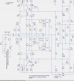
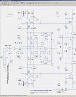
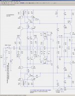
I did a quick-dirty simulation again just to show the VAS standing current responding the changes of a transistor in the IPS.
The first picture is before the changes, everything matches, the VAS Ie@Q13 is 4.9mA, the DC offset at output (not shown) is 0.23mV.
The 2nd picture shows one of the current mirror transistors, Q9B, was changed from BC857C (BF=515) to BC860C (BF=315), causing Ie@Q13 to become 2.7mA, and the DC offset at output (not shown) 6.5mV
The 3rd picture shows the current mirror was changed back to where we started, but one of the input transistors, Q5A, was changed from BC847C (BF=524) to BC850C (BF=324), causing Ie@Q13 to become 7.3mA, and the DC offset at output (not shown) 52.3mV.
Attachments
Ranchu32,
Nice tight layout, using some smd R's in spots to save space.
With one pair of outputs, you might want to investigate MAG6332/9412 devices.
BTW, it is also nice to have a design well analyzed by the veterans
Nice to see @nattawa participating too, I was wondering how his designs are moving along as I lost track of an earlier thread.
Good luck with your project.
Nice tight layout, using some smd R's in spots to save space.
Sim would have caught that onePlease check Q13 & Q14 on the schematic you posted - they look to be incorrect.
With one pair of outputs, you might want to investigate MAG6332/9412 devices.
BTW, it is also nice to have a design well analyzed by the veterans
Nice to see @nattawa participating too, I was wondering how his designs are moving along as I lost track of an earlier thread.
Good luck with your project.
Last edited:
I am not familiar with the LED D4, how much voltage it drop to know the tail current. I assume it's 1V, so the tail current is about 1mA.I did a quick-dirty simulation again just to show the VAS standing current responding the changes of a transistor in the IPS.
The first picture is before the changes, everything matches, the VAS Ie@Q13 is 4.9mA, the DC offset at output (not shown) is 0.23mV.
The 2nd picture shows one of the current mirror transistors, Q9B, was changed from BC857C (BF=515) to BC860C (BF=315), causing Ie@Q13 to become 2.7mA, and the DC offset at output (not shown) 6.5mV
The 3rd picture shows the current mirror was changed back to where we started, but one of the input transistors, Q5A, was changed from BC847C (BF=524) to BC850C (BF=324), causing Ie@Q13 to become 7.3mA, and the DC offset at output (not shown) 52.3mV.
Can you repeat the simulation with R14, R16, R18 and R20 = 300ohm. R21, R26, R27 and R34 =1K and see how the current change.
I don't think the offset voltage is that important as this is handle by the GNFB.
BTW, what is the reason using LED to set bias? I use diode with resistor, I also design to drop about 1V across the resistor to take out the Vbe variation.
Thanks
Last edited:
It is not OK for me, I hold onto the design because because each part of the circuit is well proven to have very low distortion. It is more like putting up, making the best and try to make it work.Good point, nattawa. So a standing VAS current of 10mA +/- 50%, which seems acceptable to Alan, is asking for trouble, resulting in a highly unstable OPS bias. In such cases, one need a much more robust bias generator than a simple Vbe multiplier. To me, a variation of +/- 50% is totally unacceptable. Better to prevent than to cure. IOW, keep the VAS current as stable as possible.
Cheers, E.
I studied your circuit more last night, my understanding is you sum/subtract current between both transistors(Q4 and Q5) of the differential pair at the collector of Q9. You pull 5mA using I1 and about 1mA using Q7 to make sure Q10 always conduct current, never turn off. So Q9 operates between almost 1 to 11mA.
Question is what is the distortion? That's ultimately the most important question. This is one part I am not good at calculating. I am still trying to find transistor data for LTSpice to work on the simulation. I am willing to hand pick transistors to match if my circuit is proven to give the lowest distortion. That's what is important to me.
Also in your circuit, the VAS current gain is low, you have to use 5 mA tail current which force you to use 5K input resistance to avoid offset voltage getting too high. Is all the existing preamp able to drive 5K? I don't know, I saw a lot of people use higher input resistance like 25K.
- Home
- Amplifiers
- Solid State
- Bob Cordell's Power amplifier book