Alan, confirm the following measurement:
Vrb+Vbe+Vre
This should be identical for all 5 N devices and a different identical value for all 5 Pdevices.
Now individually measure Vrb and the respective Vre and determine the individual Vbe. And measure Vbe to confirm.
Now you can plot Ie vs Vbe. This may give some useful set up information.
Vrb+Vbe+Vre
This should be identical for all 5 N devices and a different identical value for all 5 Pdevices.
Now individually measure Vrb and the respective Vre and determine the individual Vbe. And measure Vbe to confirm.
Now you can plot Ie vs Vbe. This may give some useful set up information.
I'm not sure if R12 has that big a role to play in the thermal compensation, it's much more to do with keeping the bias spreader's voltage constant in the face of varying current through it.
In reference to Doug's use of 0R1 Re in multi-pair output stages, contrary to Bob's recommendation, this does suggest that we must be missing something in terms of the analysis presented in Bob's book. This analysis would suggest that 0R1 Re is extremely risky, in terms of the possibility of a single device in a multi-parallel-device output stage hogging all/most of the current and thereby exceeding its SOA.
Some comments in regards to this:
1. Doug has stated that 0R1 presents no problem in terms of thermal stability. This is, however, not surprising. What one might expect, in the absence of device matching, is current hogging in a multi-pair output stage. Perhaps Doug meant for the phrase "thermal stability" to cover this aspect of thermal design also, but thus far, he has not stated explicitly that current hogging is not a problem.
2. Perhaps his designs "get away with it" because audio amps are used to amplify music signals and not sinewaves. Perhaps with a 1/3 rated power sinewave test, the amplifiers would not fare so well.
3. Perhaps Bob's analysis is overly conservative and the thermal resistance numbers are much lower, giving a below unity (hence safe) thermal loop gain in the Re=0R1 case.
I find myself in the difficult situation to agree on all counts
 .
.Harry, re your observation on R12, the VAS current is set up with a current source. I would expect that is pretty constant when operating in its linear region (the VAS stage that is) into a nominal 8 ohm load. Of course, if you go pulling lots of current out to drive the OPS, then there could well be some fluctuation.
R12 essentially provides some additional 'thermal gain' that allows the compensation to bend a bit more than the 1st order comp provided by the sensor transistor - at higher temperatures this provides greater reduction in the spreader voltage.
If you are using 0.1 Ohms, the Oliver voltage dictates the bias current is set much higher, so you do get current balancing due to Iq.Re.
However, I will stick with 0.33 Ohms which I use in all my designs. I think this is a good compromise between standing power dissipation, distortion and thermal stability. I also bias by designs up higher than the Oliver criteria.
Last edited:
Edmond, can you explain why? I am not getting your point on this.
Hi Andrew,
It's a diamond driver.
Cheers, E.
edit: BTW, I get the impression that nobody has looked at this schematic.
Last edited:
Right. In addition to giving his experience here, and writing books about it, he should provide unlimited free consulting to anybody here with a personal blank spot.
You really crack me up.
Jan
Yes, for over $60 a pop, I do expect more. don't want to share the secret, do a short form cook book style and charge $20. I read plenty of books in electronics, each and every single one explain why, not just saying it just is.
You might only want the result only, but I do care.
Hi Alan,
I'm sorry to say so, but your bias generator is wrong. The main culprit is Q18, which lowers the tempco of this circuit (unless it's also mounted on an O/P device, of course). Try fig. 22.28-b of APAD6.
Cheers, E.
I can't find what is APAD6, went on Google to search and keep referring to p652 in Cordell's book. there is no p652!!!
Can you explain why Q18 lower the tempco?
Thanks
Thanks guys for all the information. I have to spend time reading the posts again and think about it.
Things I need to response in general:
1) I am using 3EF diamond. From my table shown, the pre-driver and driver compensate each other very well, it's never an issue. I only have to worry about the bias spreader compensating the big output transistor only. So I only need 2Vbe compensation.
2) From my testing last night it works really well after I change to MJW as bias spreader. I did testing with up to 1A Iq and it dropped only from 1A to 0.94 when it got really hot. I finally tried adjusting the voltage across 0.22ohm Re to 30mV (about 140mA per stage) as suggested by AndrewT a few days ago when hot. It is absolutely stable. I then turn it off and blow fan on the heatsink for 1/2 hr to go back to room temp. I measure, I got 26mV across. This is absolutely perfect. This mean adjusting to Oliver's condition when cold, it will go to 30mV hot as suggested by AndrewT.
3) I will read Mr. Cordell book on the part of compensation, I just forgot it. that's just old age.
4) I need to know why Q18 hurts the tempco, yet to find out why.
5) I am going to try lowering the Re and see whether there is hogging issue. I already make it easy to add a parallel resistor by putting the 0.22 on the bottom and left long enough lead on the top for adding the parallel resistors.
Thanks
Last edited:
I can't find what is APAD6, went on Google to search and keep referring to p652 in Cordell's book. there is no p652!!!
Can you explain why Q18 lower the tempco?
Thanks
Hi Alan,
APAD6 = Adio Power Amplifier Design 6th edition.
Culprit Q18: see post 6516.
Cheers, E.
Harry, re your observation on R12, the VAS current is set up with a current source. I would expect that is pretty constant when operating in its linear region (the VAS stage that is) into a nominal 8 ohm load. Of course, if you go pulling lots of current out to drive the OPS, then there could well be some fluctuation.
Indeed. Current through bias spreader is equal to current source current minus what goes to the output stage. Check out the device data sheets. Minimum gain for that amplifier's output stage is not that high so bias spreader current variation could be significant.
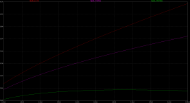
I did a quick LTspice sim. See attached, comparing R12 present and not present. X-axis is current through bias spreader, y-axis is developed voltage. I used Bob's MJE340 model but the voltage developed looks a bit high to me (this is with PR1 = 0 ohm), however the sim still shows the principle. In simulation land, voltage vs current is flattened with R12 = 150R. Of course for the "flat" case voltage developed is also lower so R12 value and developed voltage have to be iteratively optimised. I'm sure Doug optimised this in "real life" rather than the simulator!
I see now how R12 can indeed be involved in the thermal design. In this case, rather a large R12 value is required to give a "flat" voltage vs current characteristic. Other designs I've evaluated, do not requre R12 to be as large so its effect in that case is much more to flatten the V vs I curve rather than manipulate the thermal response.
Attachments
Alan, confirm the following measurement:
Vrb+Vbe+Vre
This should be identical for all 5 N devices and a different identical value for all 5 Pdevices.
Now individually measure Vrb and the respective Vre and determine the individual Vbe. And measure Vbe to confirm.
Now you can plot Ie vs Vbe. This may give some useful set up information.
I think I almost have enough information in my excel file to give that. I measure the total voltage between the two emitters of the driver transistors under column "Spreader V" for different current. I listed the Vbe of each transistor and voltage across each Re. That should almost give the information you asked. I did not measure the voltage across the base stop. But you can use the Spreader V to minus the Vbe and Re voltage out.
You can plot Ie vs Vbe, I have that written in the excel file for every single transistor. You can see they match very well except Q6 and Q17 at high temperature. At even 1A, you can see ALL match well, only when it get dangerously hot then Q6 and Q17 start to deviate off.
You are right in saying the smaller heatsink in my picture won't take high power. I cannot drive 60W, it just gets dangerously hot. No current hogging, but I suspect if I leave it on, they all going to burn!!!
I am surprised I cannot attach the excel file so people that want to, can play with it. I spent hours measuring and creating that file and all I can do is posting the jPEG image of the excel file!!! It was very hard to do the measuring, the reading change very quick, I had to really measure and write fast!!!
On pages 37 through 40 I discuss how I solved the thermal comp issue in my e-Amp here
http://hifisonix.com/wordpress/wp-content/uploads/2011/03/The_e-Amp_V2.03.pdf
Here I discuss thermal comp issue in more general terms
http://hifisonix.com/wordpress/wp-c...on-for-Audio-Amplifier-EF-Triples-V1.0231.pdf
You also explained it to me on the DIYAudio What is a CFB amplifier discussion.... which spun off at least two other designer subjects. Your description of getting/trimming the bias for constant idle was quit clear, I thought. But dont remember where in the forum it is. Glad it is also on your own web site.
It is the only such description for proper bias operation ref thermals I ever saw. With credit to you, it ought to be in every book published on audio design.
THx-RNMarsh
Last edited:
5) I am going to try lowering the Re and see whether there is hogging issue. I already make it easy to add a parallel resistor by putting the 0.22 on the bottom and left long enough lead on the top for adding the parallel resistors.
Thanks
what did you find out/learn?
-RNM
Because of saturation of Q9, that is, at high temperatures....
Can you explain why Q18 lower the tempco?
Thanks
- Home
- Amplifiers
- Solid State
- Bob Cordell's Power amplifier book