Hello all.
As some of you have become aware through my recent posts, I have become interested in sucking all the bandwidth I can out of power amps using alternate stability compensation schemes.
I'm sure this is old hat for many of you been-there-done-that guys, but looking at wiring parasitics in the simulator I realized that low-inductance traces are probably necessary to implement alternate compensation with adequate phase margin for stability.
Here is what I think I understand:
1: For a balanced line, the magnetic fields of the signal flowing in opposite directions cancel out and result in lower inductance as long as the conductors are close enough.
2: For a single conductor close to a conductive plane (IE a ground plane), the magnetic field produced by the signal will cause eddy currents in the plane with opposing magnetic fields, again canceling inductance depending on the distance to and quality of the plane.
3: Closer coupling (distance between) traces/ground plane will decrease inductance/phase shift/losses at HF but at the expense of increased parasitic capacitance.
I haven't seen many DIY PCB's using ground plane construction, usually it's just wide traces carrying rails and a ground trace. I think a few of those stratospheric low-THD amps do.
I've searched for information on this but haven't found any. Are there any online pages discussing RF PCB layout?
Thanks,
- keantoken
keantoken,
What is alternative stability compensation?
You are basically correct in what you are saying, except in item 2 the return current is not an Eddy current.
In general, you shouldn't have to worry much about wiring inductance at audio frequencies. The inductance of a piece of wire a long ways away from a ground plane is probably less than 20 nH/inch. At 1 MHz this is .126 ohms or reactance, so it won't do much because other impedance are much higher than this.
Rick
Stability depends on unity gain phase margin, which for the amps I make will be in the tens of MHz (optimistically). Small parasitics can create phase anomalies higher than this that cause ringing and instability. Electrolytics used for decoupling have their own self-resonances and this factors in with any stability compensation because the compensation currents (which matter at VHF) must travel through these caps. I want to avoid reactive ground paths so that decoupling is maximally effective.
My main aim is to have low-reactance ground return paths for the stability compensation, so that I can have stable amplifiers which are also fast. large compensation capacitors have a knack of injecting ultrasonic switching trash into the feedback loop, but alternate methods are less trivial and RF-aware PCB design should help with this.
- keantoken
keantoken,
Here is an excellent reference of RF stuff. Signal Consulting, Inc. - High Speed Digital Design and Signal Integrity Solutions Johnson has written a couple of books on this, but they are very practical and keep complex math to a minimum.
Rick
Here is an excellent reference of RF stuff. Signal Consulting, Inc. - High Speed Digital Design and Signal Integrity Solutions Johnson has written a couple of books on this, but they are very practical and keep complex math to a minimum.
Rick
"Alternative" compensation would be anything other than the single B-C cap used on the VAS in a great many DIY amps. Two-pole, Transitional Miller, Phase lag compensation, etc. would fall into this description.
I guess calling it "alternative" is a bad idea, I'll stop using that term...
EDIT: thanks for the link, looking...
- keantoken
I guess calling it "alternative" is a bad idea, I'll stop using that term...
EDIT: thanks for the link, looking...
- keantoken
Groundplane PCB design for power amplifiers is not easy. The issue is that high currents find the way of minimum resistance through the groundplane, and contaminate low level signals by EMI. I have tried several times to design power amplifier PCBs with groundplanes, and alway got worse suppression of line frequency components than with a conventional design. Groundplanes are superb for preamps, but IMO tricky for power amplifiers.
The issue is that high currents find the way of minimum resistance through the groundplane, and contaminate low level signals by EMI.
Separate ground planes for signal and power ground maybe? My concern is only for the input and VAS stage, which can be decoupled from the power stage by RC filters. Isn't this sort of the same concept as the 10R resistor used between signal and power ground for hum suppression?
- keantoken
audio frequency currents in gnd planes are mostly resistance controlled so they will "spread", on average taking the shortest path from source to sink thru the plane, regardless of the paired trace routing - happily radiating audio frequency magnetic field "in exchange" for the lower resistance path
only at really high frequencies does proximity effect result in most of the trace' return current flowing as a image in the plane
for low current Class A front end circuits a local plane could be fine but you should want to understand/use hybrid versions of "star gnd" for higher current output device power wiring - low impedance planes or fat power bus may still be right but separated by slots/constrictions from the low signal "clean" gnd plane
power output device package parasitics may be your biggest problem in reaching higher frequency gain intercept
I always like to point to the IXYS RF mosfets as potential "ultimate" feedback amplifier output devices:
IXYS RF: HF/VHF Linear MOSFETs
and the white paper:
http://www.ixysrf.com/pdf/diodes/app_notes/kelvin_lead.pdf
Last edited:
Currently I simulate with C5200/A1943 BJT outputs. I don't mess with FET stuff much, what makes a MOSFET any faster than a BJT with 20x less parasitic capacitance?
It is not necessary to have a superfast amp to reach the performances I'm looking for, just a well behaved one that is tolerant of different stability schemes. This is what I've learned in simulation at least.
So it looks to me for the moment that I want to design with both ground plane and star ground principles in mind to avoid cross-contamination of ground currents.
What about rail-plane? Same basic thing except with the rails, say each rail gets one half of the board. This way, decoupling caps can easily be placed at the crack between rails. Say the top of the board is + and - rails, half and half, while the bottom is ground plane. This way we get local decoupling everywhere through the PCB material's capacitance.
- keantoken
if you want to use more feedback you need faster output devices in negative feedback amplifiers since higher V, higher current output transistors are the usual speed limiting devices in audio amps
there is a "conservation law" for feedback systems:
http://trs-new.jpl.nasa.gov/dspace/bitstream/2014/19495/1/98-0905.pdf
that shows increasing loop gain intercept frequency is the most effective way to get larger area of effective negative feedback to use
you can also shape the available negative feedback excess gain to have more audio frequency loop gain – “2-pole” compensation is a 1st step in that direction
Mosfet are inherently faster majority carrier devices - push the charge into the gate and the drain current will change
BJT have a larger inherent "non-minimum phase" carrier diffusion time that limits their ultimate speed in feedback circuits
either are "fast enough" that fine feedback amps can be made - but Mosfets do have the speed edge even if they need more drive to realize their potential
1.5-2MHz gain intercept allows 20-30 dB more loop gain at 20KHz (and all lower audio frequencies) than your 150-200 KHz
Stability, Desensitivity/distortion reduction feedack optimization needn't be limited just to hit a amplifier signal bandwidth target
I would use the higher loop gain intercept and add input filtering to eliminate slew rate concerns and limit RF at the amp input causing IMD
Stability, Desensitivity/distortion reduction feedack optimization needn't be limited just to hit a amplifier signal bandwidth target
I would use the higher loop gain intercept and add input filtering to eliminate slew rate concerns and limit RF at the amp input causing IMD
Last edited:
1.5-2MHz gain intercept allows 20-30 dB more loop gain at 20KHz (and all lower audio frequencies) than your 150-200 KHz
Stability, Desensitivity/distortion reduction feedack optimization needn't be limited just to hit a amplifier signal bandwidth target
I would use the higher loop gain intercept and add input filtering to eliminate slew rate concerns and limit RF at the amp input causing IMD
I think around 30db and 20KHz is about right in a 'normal' design'. If you go adding 20-30db on top of that figure you are asking for trouble.
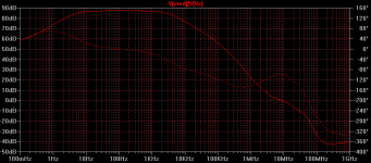
Hi,
is that graph showing ~35degrees of phase margin around 500kHz?
That big dip in phase looks wrong to me, but I am not an AC person.
Could the idea of combining planes and star routing be combined?
Allow a wide trace (part of a plane) to run under and parallel to the main flow trace and the HF components of that return current will follow the same HF components of the flow trace. This gives separation of the very different current flows and returns and also gives the low inductance due to the thickness of the PCB substrate for any HF signals.
Slots in Ground Planes
http://www.ultracad.com/articles/slots.pdf
Printed Circuit Design & Fab Magazine Online
A solid contigous plane is best especialy as the frequency goes up, but careful component layout is required, and control of where signals are routed and where the return current will go. Adding slots is not for the faint hearted and can often cause more problems than they solve.
Most examples of analogue designs with GND planes (be it either instrumentation or Audio) tend to be commercial, and as such cant be published. Also there is the cost involved, as a rule the PCB's will be 4 or more layers.
One good method of visulising the currents is to draw the current loops on your circuit diagram, using red for power, green for low power, this will help decied on component placement etc.
Hi,
is that graph showing ~35degrees of phase margin around 500kHz?
That is a plot made using two-pole stability compensation. The dip in phase allows the open-loop gain to come down steeper in order to have the same phase margin with higher corner frequency, and more gain across the audio spectrum.
- keantoken
Yes,............The dip in phase allows the open-loop gain to come down steeper in order to have the same phase margin with higher corner frequency, and more gain across the audio spectrum.
I can see that. It crosses the 0dB @ <9db/octave.
It is steeper than 6dB/octave at frequencies below where it crosses 0db.
That was not what I asked.
Is that 35degrees of phase margin at around 500kHz?
Will that phase dip affect the audio performance?
- Home
- Amplifiers
- Solid State
- Ground plane PCB design for power amps