Since I found out how to set bias current everything that confused me makes sense now. This is so embarrassing. 
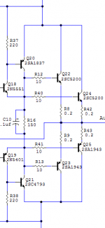
A.H. recommends to set the bias that there's a 18mV voltage drop across each resistor. With 0R22 resistors this gives 82mA through each pair of output transistors, right? So the total idle power loss with 10 pairs is around 150W???
Setting the bias made me think about the potentiometer. Given the case the wiper loses contact with the resistor the base / gate of the bias transistor is floating. With a BJT in place it stops conducting and bias current increases till the output stage dies. With a FET in place anything may happen, most likely the same. Right? In most amps I've seen the wiper of the potentiometer is connected to one of the resistor terminals and the potentiometer is located on the sinking side of the base / gate. Wiper failure in this case decreases bias current to save levels.
The downside is that the total resistance of the bias setting resistors+potentiometer circuit varies with bias settings since the resistance of the potentiometer itself is varied instead of just picking a voltage from the potentiometer.
In simulation the safe solution sometimes caused strange problems. I haven't figured out yet what makes spice go mad.
Lee
Attachments
Substitution
Hi Lee,
I would suggest to replace Q13/14 and Q8 with small TO-92 transistors, you don't need a high power TO-126 device. The 2SC2240 would perfectly fit the current mirror.
I you want a fixed voltage drop over R17 replace it by a zener diode, you could onmit the capacitor. (C12)
regards,
Piersma
Hi Lee,
I would suggest to replace Q13/14 and Q8 with small TO-92 transistors, you don't need a high power TO-126 device. The 2SC2240 would perfectly fit the current mirror.
I you want a fixed voltage drop over R17 replace it by a zener diode, you could onmit the capacitor. (C12)
regards,
Piersma
Hi Piersma
Thanks for your suggestions.
I spent some time thinking about them and also spiced a bit.
I'm not sure about this but from what I read about current mirrors I don't think it is a good idea to use dissimilar transistors in a mirror. I think the pairs Q8 + Q9 and Q13 + Q14 should be same type, preferably matched ones. I admit I haven't simulated this yet. But I will do later and also do some more research.
I'm curious how the swapped Wilson current mirror will perform in this amp. I read it doesn't improve anything drastically. It's just there because I fell in love with it on the first glimpse. It's so symmetric, nice to look at and mirrors currents perfectly.
What I like about the TO-126 is that they don't require more space than a TO-92 and are easy to couple thermally. I already updated layout and placed the current source transistors back to back. I will put a mica insulator between them and couple them with a plastic screw. For the mirror I'm not sure yet whether this is a good idea.
To change the circuit around R17 was a great idea! The Zener doesn't change performance considerably but putting the weird pnp transistor with base to ground like in the SymAsym in this palace drops thd from 0.006% to 0.0025%.
The transistor has to dissipate ~0.5W. Do you think the SA1381 will do the job? Maybe the SA1837 is better there?
This amp is becoming more and more like a high power version of the SymAsym...
By the way:
I found this reading one of the SymAsym threads:
http://www.ampslab.com/Images/bi120/bi120_schema.gif
regards,
Lee
Hi Piersma
Yes, I also think a heatsink will be required.
I simulated the CFP driver but was disappointed to see almost no difference. At least in THD. Maybe it has other advantages I don't see? It looks nice and I'd like to use it but I have no idea what makes it superior to the primitive driver in place now.
I tried another thing:
Why not stuff some more transistors into this fat amp?
So I squeezed a cascode stage into the VAS, including CCS. Another four transistors and other components that make the amp more weird. This made THD drop from 0.0025% to 0.0016%. It's not optimized yet and maybe I can squeeze more out of it.
This amp will become so high performant and thus complicated that it for sure will spontaneously burst into catastrophic oscillation and take my speakers with it to heaven.
Regards
Lee
Yes, I also think a heatsink will be required.
I simulated the CFP driver but was disappointed to see almost no difference. At least in THD. Maybe it has other advantages I don't see? It looks nice and I'd like to use it but I have no idea what makes it superior to the primitive driver in place now.
I tried another thing:
Why not stuff some more transistors into this fat amp?
So I squeezed a cascode stage into the VAS, including CCS. Another four transistors and other components that make the amp more weird.
This made THD drop from 0.0025% to 0.0016%. It's not optimized yet and maybe I can squeeze more out of it. This amp will become so high performant and thus complicated that it for sure will spontaneously burst into catastrophic oscillation and take my speakers with it to heaven.
Regards
Lee
Attachments
Hi Lee,
Because of the high amount of FET-outputdevices you will end up with a very high inputcapacitance of the outputstage. It would be beneficial to drive the outputstage with a very low impedance (Z) source that's why i suggested the CFP. But most probably the emitter follower will do also.
Did you check the stability criteria of your new creation?
It should be defenitely possible to tame this "monster" amplifier.
regards,
Piersma
Hi Piersma
Yes, the capacitance of the output stage is huge and I'd like to have a more powerful driver.
To me it seems the main benefit of the CFP is to reduce loading of the VAS further. Not sure about that.
I found an old schematic from A.H. on the net with the "AV" topology where he drives four pairs of output FETs directly from VAS. Since this worked loading of the VAS seems possible to some extend. The driver stage is only a little load there. However, someting more advanced than the EF would be nice.
By the way: With the cascode in VAS the current through VAS was reduced to the half. No idea whether this is good or bad.
Yes, I checked stability. Given I do that correctly. Attached the gain vs. phase plot. Transient response showed no overshoot except in capacitive load without output inductor network.
I'm most afraid of some unpredictable local oscillation caused by parasitics or something being hardly measurable in the 100 MHz range or so.
Any ideas to add some damping or clamping in spots that are likely to show such ill effects?
Thanks
Lee
Yes, the capacitance of the output stage is huge and I'd like to have a more powerful driver.
To me it seems the main benefit of the CFP is to reduce loading of the VAS further. Not sure about that.
I found an old schematic from A.H. on the net with the "AV" topology where he drives four pairs of output FETs directly from VAS. Since this worked
loading of the VAS seems possible to some extend. The driver stage is only a little load there. However, someting more advanced than the EF would be nice. By the way: With the cascode in VAS the current through VAS was reduced to the half. No idea whether this is good or bad.
Yes, I checked stability. Given I do that correctly. Attached the gain vs. phase plot. Transient response showed no overshoot except in capacitive load without output inductor network.
I'm most afraid of some unpredictable local oscillation caused by parasitics or something being hardly measurable in the 100 MHz range or so.
Any ideas to add some damping or clamping in spots that are likely to show such ill effects?
Thanks
Lee
Attachments
hi Lee,
Your worries about unpredictable local oscillation are valid. You have to carefully lay-out the board for this amplifier.
When i look at the phase/gain plots your margin is sufficient although i my view in "real life" the feedback cap (22pF) might be a little high.
You could consider:
1) small capacitive loading of the VAS
2) base stop resistors on the cascode
3) RC network on the front-end cascode
I guess you have to build a proto to be real sure !
regards,
Piersma
Hi Piersma
I will take care when doing the layout.
I'm not completely sure about grounding yet but have some ideas how to do it.
The feedback cap is the one from VAS back to inverting input of the input stage, right?
I considered your ideas:
1. Capacitive loading of the VAS is critical since the VAS seems to be very sensitive to capacitive load. I was very surprised what a small cap can spoil THD. I added caps there with a small resistor in series as a compromise. Actually this forms a snubber. Always good to have.
This observation maybe explains why A.H. switched to BJTs for driving.
It shows the importance of a powerful driver that is only a little load to the VAS. I'm still thinking about the driver stage...
2. Adding base stoppers to the cascode of reasonable value (470R) soon brings THD to levels higher than without cascode. This observation puts the cascode in question altogether. Maybe the extra complexity what adds risk of instability isn't worth the decrease in THD (33% relative but only 0.0008% absolute) that is lost so quickly with base stoppers.
I think I will kick the cascode from VAS. With the limited board space left layout would be really difficult anyway.
The reason I put it there was just curiosity because I read in one of the lengthy SymAsym threads it eliminates 2nd harmonics.
3. The series RC network parallel to the Zener for the front end cascode seems to be a very good idea and doesn't affect anything in a bad way. I will definitely implement it.
Thanks
Lee
I will take care when doing the layout.
I'm not completely sure about grounding yet but have some ideas how to do it.
The feedback cap is the one from VAS back to inverting input of the input stage, right?
I considered your ideas:
1. Capacitive loading of the VAS is critical since the VAS seems to be very sensitive to capacitive load. I was very surprised what a small cap can spoil THD.
I added caps there with a small resistor in series as a compromise. Actually this forms a snubber. Always good to have. This observation maybe explains why A.H. switched to BJTs for driving.
It shows the importance of a powerful driver that is only a little load to the VAS. I'm still thinking about the driver stage...
2. Adding base stoppers to the cascode of reasonable value (470R) soon brings THD to levels higher than without cascode. This observation puts the cascode in question altogether. Maybe the extra complexity what adds risk of instability isn't worth the decrease in THD (33% relative but only 0.0008% absolute) that is lost so quickly with base stoppers.
I think I will kick the cascode from VAS. With the limited board space left layout would be really difficult anyway.
The reason I put it there was just curiosity because I read in one of the lengthy SymAsym threads it eliminates 2nd harmonics.
3. The series RC network parallel to the Zener for the front end cascode seems to be a very good idea and doesn't affect anything in a bad way. I will definitely implement it.
Thanks
Lee
Hi Piersma
Changing the cap to 10pF seems not to change performance. I will try 10pF.
Final schematic is attached. Preliminary layout will take a while because I have to change some things. I found out VAS transistors have around 350 mW power loss and maybe this is too much for them to stay at reasonable temperature at elevated ambient temperature inside the amp. Junction to case thermal resistance is 18 K/W, case to ambient 90 to 100 K/W, in dense layout maybe even worse. I think I should add small heatsinks. This would be difficult in layout but more save.
Thanks
Lee
Attachments
Changes
hi Lee,
Connect the RC network between R9 and R10, try 220pF and 15-Ohms and connect the anode of D1 to R17.
The feedback cap value of 10pf is probably just a "starter", when you have finished the proto you might have to change its value again according to the amp's step repons.
regards,
Piersma
hi Lee,
Connect the RC network between R9 and R10, try 220pF and 15-Ohms and connect the anode of D1 to R17.
The feedback cap value of 10pf is probably just a "starter", when you have finished the proto you might have to change its value again according to the amp's step repons.
regards,
Piersma
Hi Piersma
The RC network makes more sense between R9 and R10. I've seen this in some amps before.
Connecting D1 to R17 is difficult. This is not a minor improvement but changes the input stage completely. I didn't succeed to get simulation running again.
What is the possible improvement?
Thanks
Lee
P.S.: Last weekend I already started assembly of the rectifier pcb.
Just imagine the diodes connected and everything mounted to the heat sink.
The RC network makes more sense between R9 and R10.
I've seen this in some amps before. Connecting D1 to R17 is difficult. This is not a minor improvement but changes the input stage completely. I didn't succeed to get simulation running again.
What is the possible improvement?
Thanks
Lee
P.S.: Last weekend I already started assembly of the rectifier pcb.
Just imagine the diodes connected and everything mounted to the heat sink.
Attachments
Hi Piersma
I adjusted the current sources the wrong way. With your suggestion it works. It's just a bit difficult to bias the whole thing because spice sometimes refuses to simulate. Sometimes it does a "damped pseudo-transient analysis" what indicates it doesn't like the circuit somehow and the result is always weird.
I don't see much difference between the two solutions. The connection between D1 and R17 makes the current through the diode flow through the tail current source as well and thus increases power loss there. The big difference is that no ground connection is required. Maybe this is an improvement, maybe not. Connecting R8 to R79 avoids ground in this path but seems no big change as well.
Since I wasn't able to set everything equally I have slightly higher current through VAS what maybe is the reason for increased THD.
Both solutions show almost equal PSRR - around 41dB. The schematic that uses the old tail ccs and only a resistor for the diode current has only ~37dB PSRR and more rapid decrease in PSRR at higher frequency.
Somehow I don't feel comfortable with the two current sources interacting with each other. I could put a resistor in layout used as a jumper to have both options available.
The bipolar cap is a good idea. I already used a bipolar cap for layout. I prefer a bipolar one over two ordinary caps in series for space reasons. I put a small film cap in parallel because the cap has very high ESR (~1R) and very high dielectric loss.
Thanks
Lee
I adjusted the current sources the wrong way. With your suggestion it works.
It's just a bit difficult to bias the whole thing because spice sometimes refuses to simulate. Sometimes it does a "damped pseudo-transient analysis" what indicates it doesn't like the circuit somehow and the result is always weird. I don't see much difference between the two solutions. The connection between D1 and R17 makes the current through the diode flow through the tail current source as well and thus increases power loss there. The big difference is that no ground connection is required. Maybe this is an improvement, maybe not. Connecting R8 to R79 avoids ground in this path but seems no big change as well.
Since I wasn't able to set everything equally I have slightly higher current through VAS what maybe is the reason for increased THD.
Both solutions show almost equal PSRR - around 41dB. The schematic that uses the old tail ccs and only a resistor for the diode current has only ~37dB PSRR and more rapid decrease in PSRR at higher frequency.
Somehow I don't feel comfortable with the two current sources interacting with each other. I could put a resistor in layout used as a jumper to have both options available.
The bipolar cap is a good idea. I already used a bipolar cap for layout. I prefer a bipolar one over two ordinary caps in series for space reasons. I put a small film cap in parallel because the cap has very high ESR (~1R) and very high dielectric loss.
Thanks
Lee
Hi Piersma
The zip file attached contains a preview of top and bottom layer with components.
I'm sorry I can't provide any really useful output from my pcb design environment. I use Mentor Graphics PADS - stone age technology.
The schematic almost represents spice simulation but I omitted the VAS loading. Therefore I split the input ground to avoid ground issues.
I added some light just for fun.
I kept the extra components from the AV amp that were kicked later. Most likely they are useless but might be handy in worst case.
Note that the heatsinks don't have contact with the pcb. They are well above and connected to the transistors only. I wouldn't recommend this with a single transistor or in mobile application but with two or more transistors it should be okay in a heavy amp (hope so). It was very hard to find a suitable heatsink at all. I'd prefer a heatsink that can be soldered to the pcb (and thus be grounded) but was surprised not to find any good one.
Most likely I won't order boards before I return from my vacation 13th to 20th. Sometimes it's good to put something away and review it after some time...
Regards,
Lee
The zip file attached contains a preview of top and bottom layer with components.
I'm sorry I can't provide any really useful output from my pcb design environment. I use Mentor Graphics PADS - stone age technology.
The schematic almost represents spice simulation but I omitted the VAS loading. Therefore I split the input ground to avoid ground issues.
I added some light
just for fun. I kept the extra components from the AV amp that were kicked later. Most likely they are useless but might be handy in worst case.
Note that the heatsinks don't have contact with the pcb. They are well above and connected to the transistors only. I wouldn't recommend this with a single transistor or in mobile application but with two or more transistors it should be okay in a heavy amp (hope so). It was very hard to find a suitable heatsink at all. I'd prefer a heatsink that can be soldered to the pcb (and thus be grounded) but was surprised not to find any good one.
Most likely I won't order boards before I return from my vacation 13th to 20th. Sometimes it's good to put something away and review it after some time...
Regards,
Lee
Attachments
Nice schematic, look at my Zesilova? 2 x 50 ÷ 500W aneb 100 ÷1000W
Last edited:
Nice schematic, look at my Zesilova? 2 x 50 ÷ 500W aneb 100 ÷1000W
Hi Federmann
Your schematic is drawn in a very confusing way what makes it difficult for me to follow your thoughts. The results from Google translator are funny to read but I have to guess what you wrote.
However I took a look at your work.
Except the output stage the amps have nothing in common.
Have you simulated or built this amp?
There are many strange things that make me doubt it works at all. If it does performance should be very poor.
Maybe you should open an extra thread to discuss your amplifier there.
Regards,
Lee
- Status
- This old topic is closed. If you want to reopen this topic, contact a moderator using the "Report Post" button.
- Home
- Amplifiers
- Solid State
- another one to build an AV800 / AV1000