I'm making an amplifier around LME49810 integrated driver and lack some knowledge to properly design output stage. Output stage is based on 4 pairs of MJ21193/21194. What I don't know is do the drivers need to have their emitters connected to each other via resistor, or maybe two resistors with their midpoint connected to output node ?
If so, how to calculate the value of the resistor(s) ?
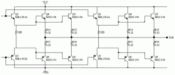
The schematic is attached.
Thanks in advance for any help !
If so, how to calculate the value of the resistor(s) ?
The schematic is attached.
Thanks in advance for any help !
Attachments
resistor suggestion
I'd go from emitter of Q2 to emitter of Q3 with a single resistor. That will give the most efficiency as you drive high levels and high frequencies. It prevents the potentially disastrous simultaneous conduction.
As to value...If you were driving a single output device, then I'd use 100 Ohms for R???. Since you are driving four in parallel, I would use 100/4=25 Ohms. That means you have to push another 1.4/25=64 mA of driver current in Q2 and Q3, and do so all the time. That further means that Q2 and Q3 need heat sinks, but your were probably planning on that already. As a side benefit, it keeps the drivers in a good place for Ft, which might help overall stability.
If you found that the high freq/high level cross conduction wasn't a problem with 25 Ohms, you might increase the value while you monitored the efficiency, but don't go too high...e.g. not above 100 Ohms.
I'd leave the circuit as is, without base resistors on the output devices.
A couple of concerns about the output stage biasing, though:
a) For least distortion, you probably want a voltage drop of about 25mV (or maybe more) across each of the emitter resistors. That means at least 100mA idling current per pair, or 400mA total idling current for the whole output stage. That's great if your heatsinks are up to the task, otherwise think about increasing the resistors from .22 ohms to maybe .47 or 1 ohm to get the idling current you want.
b) A problem with using parallel output devices is that the base-emitter voltages are not very well matched. Variation between the devices could be anything from tens of millivolts up to a couple of hundred on a bad day.
At high output currents, they'll still share the load nicely, but at idle, or low output, you might find one hogging most of the bias current while the others are loafing. That gives you worse distortion at lowish levels, as some of your output devices are only switching on when you reach, say half a watt of output.
So: matching the transistors is a good idea. If you're building more than one amp channel, you can swap them around to get as best a balance in each channel as possible e.g. all the high-bias-voltage ones in the left channel and all the low-bias-voltage ones in the right channel.
Another option is to double up on the driver transistors as shown in the diagram (or even use a separate driver for each output device). At first this makes things worse, because now you have Vbe mismatches in the driver transistors as well. However, you also have more choices for swapping around. i.e. use a low-Vbe driver to drive a couple of high-Vbe output devices and vice-versa.
btw: I agree with djoffe regarding resistor values for the driver-stage biasing (and using a single resistor between the emitters rather than two).
A bonus with doubling up on the drivers is you're also doubling their (combined) idling current to help with output-transistor switch-off speed, and running them cooler too at high output levels.
*oops - just noticed I drew the resistors as 100 ohms each - should probably be lower - e.g. 22 or 47*
Sorry if that was a bit long, hope it helps.
ps: hope you're putting Q1 on the same heatsink as well!
Attachments
I know that 3281/1302 are overkill, but some people have measured that performance of LME49810 driver chip degrades with higher output currents so I'm trying to lower the current from driver chip by using higher gain of 3281/1302 pair.
Do you think that I should stick with 15032/15033 and that advantages of using 3281/1302 will be negligible (if there will be any) ? Any advice is appreciated.
Do you think that I should stick with 15032/15033 and that advantages of using 3281/1302 will be negligible (if there will be any) ? Any advice is appreciated.
..What I don't know is do the drivers need to have their emitters connected to each other via resistor, or maybe two resistors with their midpoint connected to output node ?
If so, how to calculate the value of the resistor(s) ?
The schematic is attached.
Thanks in advance for any help !
Err, this might sound dumb, but I fail to understand why a resistor is needed in this location. Is it to provide some kind of stability?
thank you
- Status
- This old topic is closed. If you want to reopen this topic, contact a moderator using the "Report Post" button.
- Home
- Amplifiers
- Solid State
- Need help with output stage