Hi,
from many top class operational amps there are schematic diagrams at botton from the datasheets (e. g. AD797, see
http://www.diyaudio.com/forums/attachment.php?s=&postid=1090297&stamp=1167126984
For the newest LME series from National Semiconductor I don't find schematics by concerning datasheets. I find on other places a wide range of information sources e. g. about
http://www.diyaudio.com/forums/showthread.php?threadid=86276
http://www.diyaudio.com/forums/showthread.php?threadid=132471&perpage=25&pagenumber=1
but also no schematic diagrams of the internal structure. Who is the developer of the LME design?
Perhaps one of you can give me advice about download source of this one.
Thank you very much in advance.
P.S. The main reason for the high sonic quality of AD797 (by the way - also by Mr. Nelson Pass power amps from X-Series, basicly bridged AD797, main difference: MOSFETs and power follower output version) is the single voltage gain stage as differential folded cascode.
Is it the same reason also by the newest LME series`?
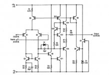
I have read this patent document:There's no schematic because National don't want to tell their competitors how they've done it. Duh!
Boliven Patents - US7071781: High speed, high resolution amplifier topology - Reader
And I do not rule out the possibility, that this could be the internal circuit
He's active here as well, but he doesn't give away any secrets. Not a hint.You can go to audiokharma and search the thread "National opamp inflation" where you will meet audioman54. He is the one you are searching for.
Interesting to know ! Please let me know his diyaudio member name to reading his threads (the "audioman54" here must be an other member than that one fromHe's active here as well, but he doesn't give away any secrets. Not a hint.
http://audiokarma.org/
Last edited:
This I have done several weeks ago.Why don;t you contact National Semiconductor directly and ask them?
Nobody do understand what I need, let alone what I need it for.
Probably only very young engineers work there and first-class analog technicians and developers like Mr. Scott Wurzer (Analog Devices) are no longer available at TI.
National Semiconductor in the old form is history, too.
I think, Analog Devices together with Linear Technology should be preferred to TI concerning integrated OP-AMPs.
Internal circuits always available, if not show in the datasheets.
Last edited:
There's no schematic because National don't want to tell their competitors how they've done it. Duh!
Competitors who know how to turn schematic into silicon also know how to turn silicon into schematic. It had to be a marketing decision to avoid drama. Some people would be disappointed if they knew.
Should I post it?

Hint: it was National's tribute to a certain oldschool series of amplifiers originated by Raytheon Corporation.
YES PLEASE !!!!
but you certainly know, that a (plain, siplified) circuit tells only 1% of the story. 99% of performance of a part can be the process.
GBW of some worst case OPA circuit (at given biasing) can be easily altered by a factor of 100 by choice of an expensive (bipolar) process.
I think the biggest part of the performance boost (THD, GBW vs. power figure of merit) of audio OPAs in the last two decades comes from introduction of better and better, but and still cost effective processes.
But please post the LME schematic, if you have it !
NSC/TI processes
The process used by NSC is pretty likely one of the processes listed in the following document:
https://www.ti.com/lit/wp/snoa843/snoa843.pdf?ts=1600682727414&ref_url=https%253A%252F%252Fwww.google.com%252F
Rather likely the VIP3 process or a derivative of it.
What still puzzles me, is the fact, that the LME OPAs have so extremely low input bias currents of typically 10nA, which suggests high perfromance input bias cancelling circuitry of a precision OPA like the one used in the LT1028.
So I'm not the only one who cares, glad to know
I was thinking along the lines of 455x-456x but your guess wasn't wrong, all of them are topologically similar.
There is a number of improvements, like a follower-enhanced mirror and the follower is biased with an active source rather than a resistor and so is the follower enhancing the VAS, and all bias sources are follower-enhanced mirrors too. These are nice touches which contribute to accurate input stage balance for lower distortion and DC offset.
Also Baker clamps all over the place and the output is a diamond buffer.
Input bias cancellation is a good guess when the bias spec is too good to be true, considering the low voltage noise which normally requires relatively high IPS current. Their voltage noise is close to NE5534 but input current is much less and yet input current noise much higher. That makes no sense.
Indeed, they use a scheme similar to OP27 et al (including LT1028), but in those opamps the cancellation circuit is meshed into the second differential stage, and here no such stage exists, so it's done differently. Like in the OP27 family, some/most/? of the cancellation noise is common mode and ought to be cancelled by matched source resistances, albeit they didn't degenerate the mirror which injects cancellation currents into the pins so extra noise may come from here. I think bias cancellation and maybe good Early voltage is responsible for low distortion from mismatched source resistance, as reported by Self. The IPS is not cascoded.
If you wonder how I know such things, I have this chip under a microscope here. A good chunk of the schematic is already drawn, but I would like to complete it as much as possible. I still hope to figure out some way to measure/estimate internal bias currents, by exploiting weird behaviors outside the operating common mode input rating. We shall see.
And I still have no idea how it avoids phase reversal, but I have heard that it does. Will need to test myself. The behavior when the inputs are taken near the negative rail is quite complex, involving important transistors going into saturation or cutoff and disturbed operation of a bias mirror. Crazy stuff.
- Status
- This old topic is closed. If you want to reopen this topic, contact a moderator using the "Report Post" button.
- Home
- Amplifiers
- Solid State
- Where are intern. schematic of LME49710 LME49720 and LM4562 (LM 4562 LME 49710 49720)