Member
Joined 2009
Paid Member
Nice plot !
I see the roll off in the solid line and the 90deg phase shift in the dotted line. If I understand properly the bad news comes at 180 degrees and this doesn't happen until 5MHz where I imagine the gain of the amp is well below unity. Why would I pick this frequency, for example, why not roll off earlier ?
I think there is something important about where the HF feedback comes from. I've only read about the claimed purpose as better stability against nasty speaker loads but I'm wondering (don't laugh) if there's another factor because the VAS won't have any cross-over distortion. Hopefully the output doesn't either, but what remnants might exist there would then enter the NFB loop ?
I was reading this just now: http://www.dself.dsl.pipex.com/ampins/dipa/dipa.htm and it mentions the importance of picking the feedback point to avoid picking up cross-over currents. It also discusses the trade-off between LTP balance and 2nd harmonic. These things are starting to look more familiar now. It also introduced me to 'blameless' (I like the name!). I was curious to see a diode across C2 (in the last schematic) - what function does this serve ?
many thanks...
Why would I pick this frequency, for example, why not roll off earlier ?
That might degrade slew rate and "slow the amp down"
at or below 20k (audio).
I think there is something important about where the HF feedback comes from. I've only read about the claimed purpose as better stability against nasty speaker loads but I'm wondering (don't laugh) if there's another factor because the VAS won't have any cross-over distortion. Hopefully the output doesn't either, but what remnants might exist there would then enter the NFB loop ?
That is very good reasoning, BG ! I have seen small "artifacts"
of Xover distortion enter my perfectly balanced LTP's. GNFB
"corrects" them and I end up with my super low THD .. BUT -
what if this introduces higher order harmonics into
the LPT. In The aska way , only the pure class a VAS is
NF'ed back to the input stage. Here you might have slightly
higher high freq. THD , but no Xover"garbage" from the OPS
gets into the loop.

feedback point to avoid picking up cross-over currents
This is the "physical" part of design , try to make your takeoffs
and at the exact midpoint of your
output trace , hopefully Xover (current) transients will cancel
out. Same with your ground returns to the central grounding
point .(attached) (ps.. that board is a blameless or a aska
or any thing in between).
and the diode.. that is if you don't want to use a non-polarizedI was curious to see a diode across C2
cap , so no "pop"
 if it gets reversed biased. I use
63v non-polarized so it is a non- issue with my designs.
OS
Attachments
Member
Joined 2009
Paid Member
Member
Joined 2009
Paid Member
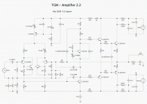
I'm probably spending too much time with the circuits instead of building because now I'm not sure I will be satisfied with version 1 given the knowledge gained. By borrowing from the FrugalAmp LTP, the Blamess protection diodes and many others the version 2 is simply more interesting - providing that the LTP 'balance' control still allows me to inject a bit of low order harmonic 'colour' into the results should I wish.
I also have to remember to scale back to lower supply rails for the final implementation as I don't need 50+W for the HT (but would like the design to be future-capable of 50+W).
I have to sort out a power supply and other things before I think about a pcb plus MJL21193 has kindly provided one of his obsoleted Patchwork Amps that will allow me to make some interesting comparisons between design elements.
I have noticed a common topology with pcb's so far so there must be a lot of proven 'wisdom' to leverage from. What are the pro's and con's of making up a simple home-pcb compare to struggling with proto-board for making up first prototypes ?
Attachments
What are the pro's and con's of making up a simple home-pcb compare to struggling with proto-board for making up first prototypes
I'm on "round" 3 &4 (pairs of amps), with the PCB you might
"get it right" the first time and keep them. Worst case you can
"regurgitate" the parts for your next one.
If you use MJL's HCL/peroxide etchant, a 4 X 6 costs 4$
and a 6 X6 costs 6$ (full price- PCB/ one sheet design/+etchant).
You might luck out and be satisfied with your first creation.
PS . R43 would be the one to affect "balance" "P3" will mostly
just offset the DC component in your output.
OS
Member
Joined 2009
Paid Member

Member
Joined 2009
Paid Member
Member
Joined 2009
Paid Member
Member
Joined 2009
Paid Member
Member
Joined 2009
Paid Member
Lumba Ogir said:I would remove C14. Nice box.
I've messed around with schematics so much that I should double check that you mean the lag compensation cap on the VAS ?
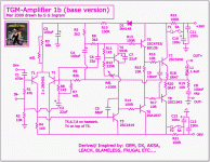
My plan is to try and reproduce the 'magic' of AKSA 25W for the first go around based on the TGM1 design (try the TGM2,3 later). That design used a lag capacitor as far as I know.
Here's a cleaner schematic of what I am doing. You will see that I am incorporating the power supply - I plan to use a single EI-style transformer on each channel:
Attachments
Bigun,
Yes I do, in post #48. I would remove C14 and keep C6.I've messed around with schematics so much that I should double check that you mean the lag compensation cap on the VAS ?
It`s going well, actually, you are about to make it better.My plan is to try and reproduce the 'magic' of AKSA 25W for the first go around based on the TGM1 design (try the TGM2,3 later).
Member
Joined 2009
Paid Member
Which one, A or B ?
I'd like some advice/opinions on power supply philosophy. I will have 5 channels in total for my HT system and I have set a budget for the transformer. I have sensitive speakers that really should do fine with a 25W/ch design. I have narrowed it down to two options and I'm not sure which is best:
A) a single Toroid, roughly 300VA with AC output fed to all of the channels in parallel which will each have their own rectifier/capacitors. I should get reasonable isolation between channels and it allows whichever channel 'needs' the most current to draw it from the main transformer. It gives me a bit more choice on voltage but for 25W I need only 18V AC. If I want more headroom I could use up to 24V AC.
B) a separate EI transformer for each channel, pcb mounted 56VA with 18V secondaries. Higher power levels and voltages for pc mount are not available (or practical) as far as I can see but this should be enough for a 25W channel. Total price is the same as for a single Toroid. I should get excellent channel isolation, building each channel as a complete 'mono-block'. The design would keep the high currents away from the input stages of the amplifier and the transformer will be oriented to 'point' it's magnetic leakage away from the board. I consider dual-bobbin EI transformers to be superior to Torroids for rejection of HF noise. I should point out that a large transformer for each channel is not justified in terms of cost and power required.
Member
Joined 2009
Paid Member
I have seen the use of two rectifiers before, but hadn't thought about the benefits. I assume it's as simple as halving the ripple noise because the voltage across each rectifier is only 18V AC instead of 36V AC. Digikey has only a few choices of slow recovery diodes and no full bridge rectifiers labelled as slow recovery (dual diodes are available only in common cathode if also slow recovery?) so I'll have to buy 8 devices per channel. I have an enquiry into another supplier that makes a full bridge using slow recovery diodes.
I understand that these diodes benefit from heat-sinking and the ones I have chosen do have metal tabs for this purpose. The good news is that I have found some abandoned heatsink material locally. Extruded aluminium, flat on one side with fins on the other, although the fins are not that long. There are 5 pieces of this stuff, each about 8 foot long and 6" wide. I took two home yesterday that I can cut up to suit the job.
It's more work than I thought going from schematic to pcb. I have to choose the components based on availability, performance and to some extent cost, in order to know their footprint and essentially do a mechanical & thermal design before I design the pcb. The electrical design is just one part of the challenge.
Member
Joined 2009
Paid Member
Member
Joined 2009
Paid Member
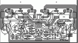
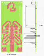
First Draft PCB (probably full of errors)...
I will keep the lag comp capacitor as an option on the pcb. I will try to design the pcb to reflect all the optional components up to version 3 of the layout but I can construct it as option 1 to begin with. The main difference is that the later version adds the LED based current source for the LTP and beefs up the LTP with supporting devices.
I don't see a problem using lots of diodes for the power supply, they're not so expensive.
This project is turning into a lot more work than I thought because I have to end up with something that accommodates 5 channels in my box. However, I think I've got a first draft on the layout. It's a single pcb per channel. A heatsink is bolted on the back-side of the board (not in direct contact of course) and adds some stiffness. The devices to be cooled are sandwiched between the heatsink and board. There will be over-sized holes in the pcb to allow me to bolt the devices to the heatsink.
The attached drawing shows preliminary pcb and side view of stack up. I don't claim 100% originality, it draws on those that have gone before and left traces of their designs on the web... to whom I am most grateful !
Attachments
Bigun,
You won`t regret it. Which type?I don't see a problem using lots of diodes for the power supply
- Status
- This old topic is closed. If you want to reopen this topic, contact a moderator using the "Report Post" button.
- Home
- Amplifiers
- Solid State
- TGM Amplifier ?