The Andrew is correct. The R20 resistor role is to improve bias thermal stability.
As far I remember I was not using that resistor in this amp (maybe I have short memory).
In my EF3 OPS this resistor was indeed improving the thermal behavior but it was also causing OPS oscillations (in that case it was not a good idea).
Remember that You can also adjust the thermal compensation by changing the R14 and R13 values (they go in parallel with bd139), or plan B is use mje340 instead of bd139 it has lower tempco.
BTW the R14 and R13 network was for the IRF Vbe, here the value of R13 will have to be lowered to get the OP transistors biassed up.
Cheers
To me getting more and more complicated (or confusing)
These was Boris answer
Greetings
Gabor
I just ran a simulation on the Borys Darlington Amplifier with the bias spreader modified, deleted the controversial resistor and also C17. Augmented R23-R24 to 0R47, as per Banat suggestion, placed an MJE340 where the BD139, adjusted TR1 to have offset 1mV, and set OS IQ to 75mA.
It is a good circuit that puts a clean +/- 30V (8R) from a +/- 36V supply, with THD in the 0.00 range. It looks like it surely will work at the first attempt.
Cheers
J.
Attachments
Last edited:
the added Hawksford/Hagerman/Self resistor is NOT for Thermal stability.
It corrects for changing current flowing from VAS to it's current source.
This VAS to Source current passes through the Vbe multiplier.
If the multiplier "through" current is always perfectly fixed at the design value, the added resistor would not be required.
The output stage draws some current from the VAS and injects some current into the Source. This extraction and injection if perfectly equal would only reduce the amount of VAS current passing through the multiplier. and the multiplier current would still be a fixed non changing value.
BUT!
the current into the output stage and injected back are not always equal and they vary, a lot. Selecting hFE of the pre-driver and driver helps reduce the variation when the amplifier is in the quiescent state. But once AC output current flows the hFE balancing no longer works for us.
At high load currents, the BJT upper base current will draw a big current from the VAS and the lower BJT base current injection will also be big. There is no mechanism to make these two draw and return currents identical at all times. Even a mosFET output stage has variable current draw and injection due to base capacitance which has to be charged and discharged.
The added resistor is there to help the Vbe multiplier to tolerate changing "through" current, not for thermal stability.
Last edited:
Member
Joined 2009
Paid Member
I did try this ...r22 connected to junction between 22R and Q5C.....
It's on a post somewhere on this thread I think. With the resistor the bias current varied much less especially at high output bias current. With about 100mA bias the bias started rising fairly rapidly with a moderate heat sink. With the resistor the rise was significantly much less. Stable I'd say. Look for the post early on in the thread.
Can't remember exactly what I said but that it worked well enough for me. I can test it again sometime. I'm out of town and down with a cold ! Not sure when I can do the test.
Because R22 purpose or where or how exactly connect was not cleared it is missing from the layout like from the last circuit simulated and posted by Mosquito (asc. file)
These has two pair darlington option
Please pay att. these layout was NOT TESTED!
Q7, Q8, Q9 and U1, U2 must be mounted from the copper side in other word will goes under the PC board
The two Foil capacitor value can be up to 10uF, R10 connect the signal GRD to the main GRD, U must use that or use a jumper to connect the two ground, J= jumpers
Greetings
Attachments
This might be a stupid question, but wouldn't you ideally split R20 between the top and bottom (i.e. one half below R13/Q9/C17) in the interest of output stage symmetry? Or is the effect too small to warrant the effort?
Error:
In my previous post I wrote R22 instead R20 that is wrong! 22R is the value of the resistor..
I don't know. The best think would be to be built and tested that way.
It is a big confusion, Mosquito did simulated and got horrible result with R20 plus a diode how it was suggested R20 to be used.
I did asked Borys who designed and built these amp with Toshiba mosfet and sound and works great.
He wrote R20 is a mistake he never used it!
Also I know these type of circuit with mosfet power devices more stable than BJT, Darlington.
I did not built these circuit yet but my old circuit which is similar to these it was unstable thermally even do I got the best sound out of the amplifier or any amplifier ever built or had in my system over 25 years or so. Believe me I built a way over 100 different circuit.
Before you draw a conclusion I must let you know I used all boutique parts and spent countless hours to find (match the parts to each others) best components and semis to get the best sound out of these little amp.
I did not gave up on these, right now I'm busy with these modules HPA-NXV500L Lateral MOSFET Amplifier Module – Holton Precision Audio
Greetings
Hi
Guys it may sound very stupid but I am tempted to use these Hitachi power device to replace the TIP type of power darlingtos...
Any constructive opinions, comments are welcomed
HTTP 301 This page has been moved
Can these device replace those darlingtons with minimum or no adjustments?
Greetings
Guys it may sound very stupid but I am tempted to use these Hitachi power device to replace the TIP type of power darlingtos...
Any constructive opinions, comments are welcomed
HTTP 301 This page has been moved
Can these device replace those darlingtons with minimum or no adjustments?
Greetings
Hi Andrew
The Hitachi datasheet I posted with my question, to met opens but I add it again with the complementary
HTTP 301 This page has been moved
HTTP 301 This page has been moved
I post the TIP147 & 142 so it will be easier to look it up.
http://www.st.com/content/ccc/resou...df/jcr:content/translations/en.CD00000914.pdf
The amplifier schematic one page back post 582
The reason I do not post direct I have an old LTspice IV software when I open with that the darlington devices are missing.
You may have something better
My question remain can I use those Hitachi devices to replace the TIP..
Greetings
Hi gaborbela,
I can't see the schematic, but you can't replace a darlington transistor with a normal transistor. You would need to adjust your bias circuit to compensate for the different Vbe drop. The other change will be that the Vas sees a greater load variation because the current gain is lower. If they are both darlington types, then the change should be pretty easy. I don't know of any Japanese darlington audio outputs though.
-Chris
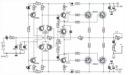
Here is a similar circuit and at the same time with a different front end.
I think it would be worth to simulate and tweak if it need to be.
Very likely the feedback resistor(s) needs to be readjusted and some adjustment around the VBE.
If someone has some time to put this little amp into the sim program that would be a great help.
For the BDW darlingtons we can use the N American version TIP 142/147 type in case someone think that would be hard to find.
Attachments
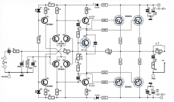
I made an error in the circuit, BDW93C & BDW94C only to be used at Max 30 V rail voltage with decent bias!! Here is the corrected circuit BUT be aware this was NOT tested neither simulated.Here is a similar circuit and at the same time with a different front end.
I think it would be worth to simulate and tweak if it need to be.
Very likely the feedback resistor(s) needs to be readjusted and some adjustment around the VBE.
If someone has some time to put this little amp into the sim program that would be a great help.
For the BDW darlingtons we can use the N American version TIP 142/147 type in case someone think that would be hard to find.
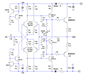
For simulation I ask for help if someone has a little extra time. I will pot one more circuit (I like that better) for simulation purpose.
Thank you!
Attachments
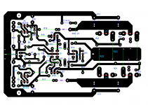
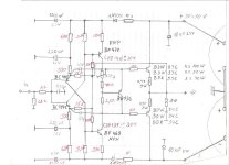
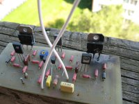
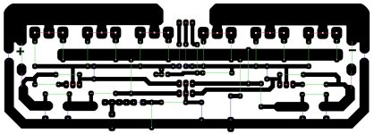
At the weekend I had some extra free time so I went back to my old good sounding amplifier. I wanted to know what lead to the disaster, thermal runaway (the amplifier blew up). My time was well spent because I found the source of the problem. The amplifier schematics was corrected and that correction resulted the Miller capacitors were not doing their job. Here is the blown up amp picture and the faulty circuit. The circuit later was corrected but the PCB layout never. On the weekend I corrected the layout (after I found the problem) I drew a new layout with 3 pairs of power darlingtons. Just remind you I am not set up with scope I could not test it on a scope.
Attachments
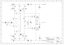
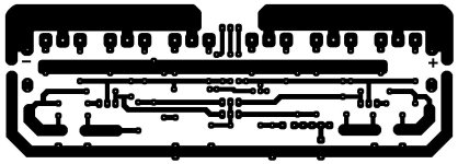
Here is the corrected circuit and the newly drawn layout! This should work without any issue! Very soon I will test it. The Layout (black and white) is mirror imaged (ready for an iron transfer) It will need to be scaled into a size where the power transistor feet fits perfect into the PBC. At the moment I am out of black in from my printer so I could not do a print it out to scale it! If the quality of the layout att. not good enough for Iron transfer that is because I am unable to post here high quality monochrome black & white pictures! Please send me a PM if you interested on better quality. Soon I will build it and test it!
Attachments
- Home
- Amplifiers
- Solid State
- My first DIY amplifier 20 years a go