Hello,
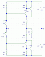
I was playing with this temperature compensating/bias voltage scheme in pspice. It allows for no adjustment of a pot to get the bias current correct, just some testing in the simulator and real life to get a good bias current set, then shes over with. The offset voltage is well below 10mV and the bias current in this one is 60 ma. It seems to be tolerant of differences in transistors as well. When I put in the simulator a ambient of 40 degrees as apposed to 27, it barely moves in offset voltage or current. I don't see this used much. Is there something inherantly wrong with it?
I was playing with this temperature compensating/bias voltage scheme in pspice. It allows for no adjustment of a pot to get the bias current correct, just some testing in the simulator and real life to get a good bias current set, then shes over with. The offset voltage is well below 10mV and the bias current in this one is 60 ma. It seems to be tolerant of differences in transistors as well. When I put in the simulator a ambient of 40 degrees as apposed to 27, it barely moves in offset voltage or current. I don't see this used much. Is there something inherantly wrong with it?
Attachments
Hi,
the bias is tied to ground. It should float with the signal level.
The two transistors are wired as diodes, quite a common compensation scheme. Adding a variable resistor between the diodes restores the adjustment.
3mA of bias in the drivers is a bit low for an output stage and keep in mind that the temp compensation has to monitor the drivers, not the outputs.
Yes, it is the same as 2 diodes. I tied it to ground at the middle to play around with the offset voltage and bias current. I didn't know it was a common scheme. I don't remember seeing it much in amps, but i have only been at this for a short while. The bias current can be changed with changing the resistors R5 and R6. A higher current there gives a higher bias current. I can reduce the resistance of R8 and R9 to increase the current in the driver transistors, but is there a better way? I just used the scheme from many amps I have seen with 200 ohms. Decreasing it to 100 increases the drivers current to 5.5ma. I was aware of the temperature monitoring just the drivers, so I figured Q12,13,8,9 would all be on a seperate heatsink together away from the larger output tansistors.
davidallancole said:I don't see this used much.
Erno Borbely used a compensation scheme like that in one of his MOSFET amplifier articles in Audio Amateur, I think around 1988.
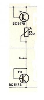
Here's the VBE Multiplier used in Borbely's first MOSFET amplifier -- and a temperature sweep. (The emitter junction was just grounded for convenience, so that everything would scale).
I didn't bother to change any of the values -- just snipped a bit for the second shot. In real life you don't want 46mA going through your VBE multiplier --
and a more conventional one
I didn't bother to change any of the values -- just snipped a bit for the second shot. In real life you don't want 46mA going through your VBE multiplier --
An externally hosted image should be here but it was not working when we last tested it.
and a more conventional one
An externally hosted image should be here but it was not working when we last tested it.
- Status
- This old topic is closed. If you want to reopen this topic, contact a moderator using the "Report Post" button.
- Home
- Amplifiers
- Solid State
- This temperature compensating scheme