what circuit is too sensitive for a conventional Vbe multiplier?xitronics said:I need a simple but effective quiescent current control circuit for my 10-watt class AB stage. Vbe multiplier is too sensitive to parasitic changes and so I find it inappropriate to make use of.
If the issue is thermal tracking, then placement is very important.Note that you have to look at the Vbe circuit in conjunction with the physical layout, so you need to indicate (picture would be a good idea) where/how the Vbe sensor is located.
I've seen a single transistor bias generator (single NPN, not even darlington) can give negative thermal compensation (overcompesation) while the output stage is triple darlington (6 B-E junctions must be compesated). The heatsink base is cooper, though

Vbe multiplier can provide controlled quiescent current to the class ab stage but cannot deal with variation the bias current source output. The collector current of class AB is a near-exponential function of the bias current. But I do agree with you all tht with a fairly stable biasing source, Vbe multiplier is a very effective solution to the problem.
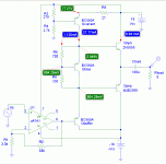
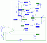
I have attached the my circuit attached to this post. Kindly suggest modifications wherever necessary.
I had another doubt.. We can use emiiter feedback resistors to set the DC collector current in class AB stage. But by adding bypass capacitors to them to maintain unity AC gain I get sharp crossover distortions in the output. Can anyone explain me why this is taking place?
________
Regards,
Prasanna.
Attachments
Your vbe multiplier isnt working correctly because the output transistors are bypassing it. Notice that the voltage at the collector and base of the vbe trans. are the same. This means no current or very little is flowing through R6. The be junctions of the output transistors are like having a jumper wire and are shunting current around the vbe multiplier. Indeed adding the driver transistors will solve your problems.
Hi, xitronics,
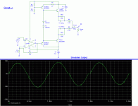
It seems without global feedback in your schematic, the output stage is much underbiased. Are you making a buffer after the opamp's output? I can think of 2 possible modifications. First, if you want to run the buffer openloop, then you will need heavy biased to force the output stage to always work in classA. Emitor degeneration is important for this first option. Second, if you want less dissipation and can afford the buffer inside the feedback loop, just change the feedback take-off point from pin6 of the opamp to the output node before 100uF. Both this may reduce the xover distortion.
It seems without global feedback in your schematic, the output stage is much underbiased. Are you making a buffer after the opamp's output? I can think of 2 possible modifications. First, if you want to run the buffer openloop, then you will need heavy biased to force the output stage to always work in classA. Emitor degeneration is important for this first option. Second, if you want less dissipation and can afford the buffer inside the feedback loop, just change the feedback take-off point from pin6 of the opamp to the output node before 100uF. Both this may reduce the xover distortion.
jerluwoo said:Your vbe multiplier isnt working correctly because the output transistors are bypassing it. Notice that the voltage at the collector and base of the vbe trans. are the same.
Hey, I have printed it by mistake.. sry for tht.. Voltage at base is 1.2V whereas tht at the collector is 805mV. Output transistors doesnt seem to bypass the source current as their bases are drawing tiny 170uA currents. I have posted the correct pic. Kindly have a look.
Originally posted by consort_ee_um
You need some driver transistors in front of the output transistors. The current demand of the output transistors will overload your current source. When you add the drivers your problem will hopefully disappear
The output transistors wont draw more than 20-25mA from the source for peak o/p voltages of upto 13 Volts. This means I can get 10 Watts of o/p without using additional drivers. But yes, current source device will dissipate power more than what a BC560-type can handle.. So i'll consider using trans with higher Pdmax.
Pls share your views on this.
____________
Prasanna
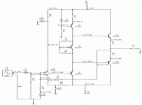
Attachments
Hi,
beside the fact you are about to blow up the VAS (or EF buffer) and it's current source, you really do need driver transistors.
Go and download the Leach paper on designing his Low Tim amplifier. He went for driver and pre-driver between VAS (buffer)and output devices.
beside the fact you are about to blow up the VAS (or EF buffer) and it's current source, you really do need driver transistors.
Go and download the Leach paper on designing his Low Tim amplifier. He went for driver and pre-driver between VAS (buffer)and output devices.
Moving your feedback takeoff point to the output would solve your problems I believe. It will remove the positive 1+ volts of offset and eliminate the crossover notches. I obtained good results with this change alone in my sims. Having the feedback takeoff at the opamp output causes the offset problem, and gave some pretty bad fourier results. I would also replace R3 with a red led and change the value of R4 to obtain at least 10mA through the led, this will give you a much better current source. I would also add a little filter for the opamp supply rails to help reject noise caused by the higher currents in the output transistors.
Attachments
jerluwoo said:Moving your feedback takeoff point to the output will remove the positive 1+ volts of offset and eliminate the crossover notches.
Ya, this circuit certainly removes output DC offset and also allows us to have greater voltage swing of upto say 15-16V as the dc bias at the current source is smaller at 511mV compared to 2.1V in my circuit. Its a nice n efficient circuit.
AndrewT said:Hi,
beside the fact you are about to blow up the VAS (or EF buffer) and it's current source, you really do need driver transistors.
This true for low-power transistors.. If I use a high-power one (although it'll raise the overall budget) the buff, source and multiplier can operate without the thermal runaway prob..
For driver stage wat do u say? Can i use a 2n3904-3055 and their complementaries in darlington config?
_______________
Pras
Hi xitronics
Your bias circuit wasn't stable because the resistor ratio (330 ohm:750 ohm) isn't correct. You need 2 Vbe's to match the output stages (2 Vbe junctions).
But you should have emitter resistors to provide thermal stability as suggested, since you can never get the compensation transistor exactly to the same temperature as the output transistor junctions.
The feedback pair stabiliser might be better : in your case you would use an NPN after the PNP, so that the PNP can operate at MUCH lower current, and then it's Vbe will hopefully be a lot closer to the Vbe's of the output transistors. The NPN then takes most of the bias current.
And you still need drivers. If we assume 16V peak output, the 2N3055/comp. have to drive 2A; they will have a gain of about 40 and need 50 mA so 2N3904/06 might be OK but you should check their voltage rating. I usually recommend BD139/BD140's as drivers because they can be put onto the same heatsink as the 2N3055/comp. and the thermal compensation works on all four at once.
cheers
John
Thanks a lot for all your advice.
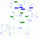
I have attached the modified circuit. In that I chose BD135/36 because PSPICE library didnt have the models for BD139/40. But BD139 offers very good Vceo and Pdmax so I would use them in implementing the ckt.
Finally, I find the need for frequency compensation. Due to global feedback, the circuit seems to have the tendency of oscillating at a higher frequency (in 100-500k range). In fact I heard it happen in another audio amp employing global feedback. Please help me in adding frequency stabilization to the ckt.
Regards,
Prasanna
Attachments
- Status
- This old topic is closed. If you want to reopen this topic, contact a moderator using the "Report Post" button.
- Home
- Amplifiers
- Solid State
- Quiescent Current Control in Class AB..?