Hi everyone,
I am trying and failing to make a layout for a diode that can take both vertical TO-220 and horizontal like 1n4007 diodes. I've seen people do it on boards, but can't find an existing layout or come up with an easy way to do that. It is basically keeping one square pad and make a duplicate further away for the second round pad on the layout. Any suggestions?
I am trying and failing to make a layout for a diode that can take both vertical TO-220 and horizontal like 1n4007 diodes. I've seen people do it on boards, but can't find an existing layout or come up with an easy way to do that. It is basically keeping one square pad and make a duplicate further away for the second round pad on the layout. Any suggestions?
Hi everyone,
I am trying and failing to make a layout for a diode that can take both vertical TO-220 and horizontal like 1n4007 diodes. I've seen people do it on boards, but can't find an existing layout or come up with an easy way to do that. It is basically keeping one square pad and make a duplicate further away for the second round pad on the layout. Any suggestions?
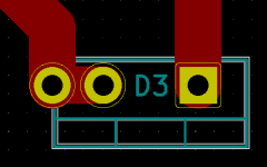
Long ago in Tango I just made multiple components for TO220V or TO22H and then use what was needed.
I had a trim pot with 2 wipers so that you could use 2 fixed resistors instead of a pot.
G²
Hi everyone,
I am trying and failing to make a layout for a diode that can take both vertical TO-220 and horizontal like 1n4007 diodes. I've seen people do it on boards, but can't find an existing layout or come up with an easy way to do that. It is basically keeping one square pad and make a duplicate further away for the second round pad on the layout. Any suggestions?
I just went into KiCad and looked up TO-220 and they have 2,3,4,5,7,9,11 or 15 pin pin vertical, horizontal with
tab up or tab down.
G²
One of the neat things about KiCad is that if you have multiples of the same pin in a footprint, KiCad is clever enough to connect the net to all of them, so for that one you just create a component (start with the TO-220 footprint) and add extra pads. Number them the same as the pads that are already there and they get automagically connected in parallel.
One of the neat things about KiCad is that if you have multiples of the same pin in a footprint, KiCad is clever enough to connect the net to all of them, so for that one you just create a component (start with the TO-220 footprint) and add extra pads. Number them the same as the pads that are already there and they get automagically connected in parallel.
But no so good if you accidentally mis-number two pins the same ?
I would have thought even a basic syntax check would throw that out as an error.
I briefly tangled with Kicad.
As it does sheets one thing it does is when converting to a pcb puts components in a line along top of pcb. Well, ok I guess.
Until you realise you lost any layout of closely associated components from the schematic! Someone seriously fell asleep on that one.
Last edited:
Pick up a component in PCB while your schematic is open. You'll see it highlighted. It's really straightforward to place.
And it's fantastic being able to have multiple pads with the same number. Now I can have connectors (like for example the Keystone 7795, which has four pads on the PCB for one connection) without having to build a specific schematic component. I just use a normal 1 pin connector in schematic, and label all four pads pin 1, and off I go.
And it's fantastic being able to have multiple pads with the same number. Now I can have connectors (like for example the Keystone 7795, which has four pads on the PCB for one connection) without having to build a specific schematic component. I just use a normal 1 pin connector in schematic, and label all four pads pin 1, and off I go.
- Status
- This old topic is closed. If you want to reopen this topic, contact a moderator using the "Report Post" button.
- Home
- Design & Build
- Software Tools
- KiCad combined diode layout