Be interested to know where that is in the thread, all I see is people trying to be helpful...certainly MUCH more useful than a snide retort
Tip for using library generators (any type, any package) - if they can generate most of what you want (be it a symbol or footprint) you can then use that and finish it off. I use the KiCad one for footprints, even if it cannot do all the pads, I will use it to do most of the work, and add in anything that is missing manually.
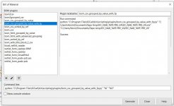
OK...I did as recommended and "bit the bullet"---downloaded KiCad v 5.1.6 and went through the DigiKey tutorial. WHEW!! Not exactly easy! But I have managed to draw a successful schematic, make parts and footprints, make a PCB layout, and generate zipped gerbers. VOILA!! The next part---the BOM---is stumping me. I can generate a csv file, but can't read it in Excel. How do you do this?
The BOM can be a nightmare.
I have had better luck importing a CSV file using LibreOffice Calc. It just works in LibreOffice, but can be a pain in Excel.
LibreOffice is free, and can be installed along side Office/Excel without any problems. You can create Excel files with LibreOffice Calc.
I have had better luck importing a CSV file using LibreOffice Calc. It just works in LibreOffice, but can be a pain in Excel.
LibreOffice is free, and can be installed along side Office/Excel without any problems. You can create Excel files with LibreOffice Calc.
Never had any luck with XML into Excel (or importing many data formats like CSV without some fiddling needed). Libreoffice Calc always works perfectly on CSV files. Even works better on some Office files than modern Office versions do.
Plus, if you put some effort in, you can customise the plugin on KiCad. Then it always generates consistent BOM files without any effort needed from any project created. Means you get the same style BOM all the time, even when components have inconsistent property fields.
Plus, if you put some effort in, you can customise the plugin on KiCad. Then it always generates consistent BOM files without any effort needed from any project created. Means you get the same style BOM all the time, even when components have inconsistent property fields.
Hi Kevin! How do you do that? My KiCad version (5.1.6) only provides cvs format in the generate BOM tool.I just save them in xml format and import into excel with no problems and save as xls or xlsx as desired.
It's CSV (comma separated values) but saved in an xml format and it can be imported directly into excel without problems, and saved as an xls or xlsx format file.
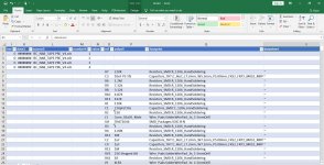
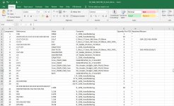
This is another tape amp project and I have not populated the parts with much detail, but you get the idea.
The python scripts in general are pretty lousy, but there are ones you can download and install. I find not all of them work correctly even the ones bundled with KiCad. I usually end up having to do a lot of clean up, in theory it should be possible to generate much better BOMs but that requires Python skills I don't possess.
Attachments
I've installed another BOM manager, KiBom which is very configurable. Generated a CSV and imported into excel. I'll be modifying it a bit.. I will probably reconfigure it for xml format.
GitHub - SchrodingersGat/KiBoM: Configurable BoM generation tool for KiCad EDA (KiCad EDA - Schematic Capture & PCB Design Software)
A couple of minutes and this is a fairly usable if not particularly pretty BOM. What get's listed is highly dependent on what you add to the part attributes. (Description, Vendor, MPN, Supplier, Supplier PN, etc.)
Attachments
If you are just starting with KiCad, I would also recommend trying Diptrace. I started with KiCad and got frustrated. My friend recommended Diptrace and it is great. Best of all, you just press a button to order circuit boards. No working through what file format is used by the board house. Just click and order. Two vendors to pick from, both are excellent.
Well, I'm FAR from being any kind of mentor on KiCad, but there's a thing or two I've learned that first-timers may not find so obvious. Experienced users, please feel free to comment and/or correct me!
When first starting, define your symbols before you start drawing the schematic. Edit and define ALL the properties of your symbol whilst creating (or modifying), including the Mouser/DigiKey page of the part you plan to use, the part number, the footprint, and the price. Doing this NOW will save you from having to go back to each and every like part on your schematic later.
When first starting, define your symbols before you start drawing the schematic. Edit and define ALL the properties of your symbol whilst creating (or modifying), including the Mouser/DigiKey page of the part you plan to use, the part number, the footprint, and the price. Doing this NOW will save you from having to go back to each and every like part on your schematic later.
If you do find you have a mistake in a component late in design, as I have before, you can open the KiCad files in a text editor (I like Notepad++)Doing this NOW will save you from having to go back to each and every like part on your schematic later.
All files are plain text files, and you can search and replace, which is easier than editing each part on a schematic. I have used this many times to quickly fix a mistake, or even just change part values if I need to.
But make a backup of your files before you start.
Last year I did a KiCad project, 4 layer board, double sided silk screen, 3"x4" 8 through hole ICs and 4 surface
mount ICs, all resistors and caps surface mount. I used JLCPCB in China, emailed the files Wednesday and
had the boards the next Tuesday. 5 pieces including 2nd day shipping ($17) was $54. Since I have parts on
both sides the double silk was very helpful.
G²
mount ICs, all resistors and caps surface mount. I used JLCPCB in China, emailed the files Wednesday and
had the boards the next Tuesday. 5 pieces including 2nd day shipping ($17) was $54. Since I have parts on
both sides the double silk was very helpful.
G²
Most Chinese manufacturers, like DirtyPCB and JLCPCB that I use, it won't make a difference, by default they accept silkscreen on both sides.
If I quote with UK manufacturers there might be a small saving on small quantities of boards, but not worth worrying about, and they will likely tell you not to bother. Like status46 said, benefit of having the second silk will be more than the cost saving.
If you were making a million boards it might be worth the saving?
When you send a job to one of these low cost PCB makers, you are sharing a panel with other peoples jobs. If one of these has bottom silkscreen, the entire panel will be screened anyway.
In high volumes, you are not sharing and cutting the redundant process step saves time and money
In high volumes, you are not sharing and cutting the redundant process step saves time and money
- Status
- This old topic is closed. If you want to reopen this topic, contact a moderator using the "Report Post" button.
- Home
- Design & Build
- Software Tools
- KiCAD for beginners