Here are the corrected models and the same jig as before.
The use of the Tjp models is explained here:
http://www.diyaudio.com/forums/soft...-power-mosfet-models-ltspice.html#post4365741
Code:* * MOSFET VDMOS Models with ksubthres *For 25C * *10N20-25 VDMOS with subthreshold (c) Ian Hegglun 06 Dec 2015 .model 10N20-25 VDMOS (Rg=60 Vto={0.17-1.6m*0} Lambda=3m + Rs={0.245*(1+2.6m*0)} Kp={1.30/(1+8.3m*0)} + Ksubthres={0.095*(1+2.9m*0)} Mtriode=0.3 Rd={0.6*(1+3m*0)} + Cgdmax=100p Cgdmin=5p a=0.25 Cgs=600p Cjo=1100p + m=0.7 VJ=2.5 IS=4.0E-6 N=2.4 mfg=IH151206) * * * *10P20-25 VDMOS with subthreshold (c) Ian Hegglun 06 Dec 2015 .model 10P20-25 VDMOS (pchan Rg=60 Vto={-0.535+1.7m*0} + Rs={0.37*(1+3.4m*0)} Kp={0.995/(1+6.7m*0)} Rd=0.2 + Ksubthres={0.12*(1+3.1m*0)} Mtriode=0.4 Lambda=5m + Cgdmax=215p Cgdmin=10p a=0.25 Cgs=900p Cjo=1200p + m=0.7 VJ=2.5 IS=4.0E-6 N=2.4 mfg=IH151206) * * * *20N20-25 VDMOS with subthreshold (c) Ian Hegglun 06 Dec 2015 .model 20N20-25 VDMOS (Rg=30 Vto={0.155-1.6m*0} + Rs={0.12*(1+2.5m*0)} Kp={2.40/(1+7.4m*0)} + Ksubthres={0.09*(1+1m*0)} Mtriode=0.3 Rd=0.16 Lambda=3m + Cgdmax=200p Cgdmin=10p a=0.25 Cgs=1200p Cjo=2200p + m=0.7 VJ=2.5 IS=8.0E-6 N=2.4 mfg=IH151206) * * * *20P20-25 VDMOS with subthreshold (c) Ian Hegglun 06 Dec 2015 .model 20P20-25 VDMOS (pchan Rg=30 Vto={-0.61+2.2m*0} + Rs={0.17*(1+2.0m*0)} Kp={1.85/(1+8.4m*0)} + Ksubthres={0.105*(1+5m*0)} Mtriode=0.35 Rd=0.05 Lambda=5m + Cgdmax=430p Cgdmin=20p a=0.25 Cgs=1800p Cjo=2400p + m=0.7 VJ=2.5 IS=8.0E-6 N=2.4 mfg=IH151206) * * ************************************************************** * For 75C * *10N20-75 VDMOS with subthreshold (c) Ian Hegglun 06 Dec 2015 .model 10N20-75 VDMOS (Rg=60 Vto={0.17-1.6m*50} Lambda=3m + Rs={0.245*(1+2.6m*50)} Kp={1.30/(1+8.3m*50)} + Ksubthres={0.095*(1+2.9m*50)} Mtriode=0.3 Rd={0.6*(1+3m*50)} + Cgdmax=100p Cgdmin=5p a=0.25 Cgs=600p Cjo=1100p + m=0.7 VJ=2.5 IS=4.0E-6 N=2.4 mfg=IH151206) * * * *10P20-75 VDMOS with subthreshold (c) Ian Hegglun 06 Dec 2015 .model 10P20-75 VDMOS (pchan Rg=60 Vto={-0.535+1.7m*50} + Rs={0.37*(1+3.4m*50)} Kp={0.995/(1+6.7m*50)} Rd=0.2 + Ksubthres={0.12*(1+3.1m*50)} Mtriode=0.4 Lambda=5m + Cgdmax=215p Cgdmin=10p a=0.25 Cgs=900p Cjo=1200p + m=0.7 VJ=2.5 IS=4.0E-6 N=2.4 mfg=IH151206) * * * *20N20-75 VDMOS with subthreshold (c) Ian Hegglun 06 Dec 2015 .model 20N20-75 VDMOS (Rg=30 Vto={0.155-1.6m*50} + Rs={0.12*(1+2.5m*50)} Kp={2.40/(1+7.4m*50)} + Ksubthres={0.09*(1+1m*50)} Mtriode=0.3 Rd=0.16 Lambda=3m + Cgdmax=200p Cgdmin=10p a=0.25 Cgs=1200p Cjo=2200p + m=0.7 VJ=2.5 IS=8.0E-6 N=2.4 mfg=IH151206) * * * *20P20-75 VDMOS with subthreshold (c) Ian Hegglun 06 Dec 2015 .model 20P20-75 VDMOS (pchan Rg=30 Vto={-0.61+2.2m*50} + Rs={0.17*(1+2.0m*50)} Kp={1.85/(1+8.4m*50)} + Ksubthres={0.105*(1+5m*50)} Mtriode=0.35 Rd=0.05 Lambda=5m + Cgdmax=430p Cgdmin=20p a=0.25 Cgs=1800p Cjo=2400p + m=0.7 VJ=2.5 IS=8.0E-6 N=2.4 mfg=IH151206) * * ******************************************************** * MOSFET VDMOS-Tjp Models with ksubthres * * *10N20-Tjp VDMOS with subthreshold (c) Ian Hegglun 06 Dec 2015 .model 10N20-Tjp VDMOS (Rg=60 Vto={0.17-1.6m*(Tjp-25)} Lambda=3m + Rs={0.245*(1+2.6m*(Tjp-25))} Kp={1.30/(1+8.3m*(Tjp-25))} + Ksubthres={0.095*(1+2.9m*(Tjp-25))} Mtriode=0.3 Rd={0.6*(1+3m*(Tjp-25))} + Cgdmax=100p Cgdmin=5p a=0.25 Cgs=600p Cjo=1100p + m=0.7 VJ=2.5 IS=4.0E-6 N=2.4 mfg=IH151206) * * * *10P20-Tjp VDMOS with subthreshold (c) Ian Hegglun 06 Dec 2015 .model 10P20-Tjp VDMOS (pchan Rg=60 Vto={-0.535+1.7m*(Tjp-25)} + Rs={0.37*(1+3.4m*(Tjp-25))} Kp={0.995/(1+6.7m*(Tjp-25))} Rd=0.2 + Ksubthres={0.12*(1+3.1m*(Tjp-25))} Mtriode=0.4 Lambda=5m + Cgdmax=215p Cgdmin=10p a=0.25 Cgs=900p Cjo=1200p + m=0.7 VJ=2.5 IS=4.0E-6 N=2.4 mfg=IH151206) * * * *20N20-Tjp VDMOS with subthreshold (c) Ian Hegglun 06 Dec 2015 .model 20N20-Tjp VDMOS (Rg=30 Vto={0.155-1.6m*(Tjp-25)} + Rs={0.12*(1+2.5m*(Tjp-25))} Kp={2.40/(1+7.4m*(Tjp-25))} + Ksubthres={0.09*(1+1m*(Tjp-25))} Mtriode=0.3 Rd=0.16 Lambda=3m + Cgdmax=200p Cgdmin=10p a=0.25 Cgs=1200p Cjo=2200p + m=0.7 VJ=2.5 IS=8.0E-6 N=2.4 mfg=IH151206) * * * *20P20-Tjp VDMOS with subthreshold (c) Ian Hegglun 06 Dec 2015 .model 20P20-Tjp VDMOS (pchan Rg=30 Vto={-0.61+2.2m*(Tjp-25)} + Rs={0.17*(1+2.0m*(Tjp-25))} Kp={1.85/(1+8.4m*(Tjp-25))} + Ksubthres={0.105*(1+5m*(Tjp-25))} Mtriode=0.35 Rd=0.05 Lambda=5m + Cgdmax=430p Cgdmin=20p a=0.25 Cgs=1800p Cjo=2400p + m=0.7 VJ=2.5 IS=8.0E-6 N=2.4 mfg=IH151206) * * **************************************************************
Thank you.
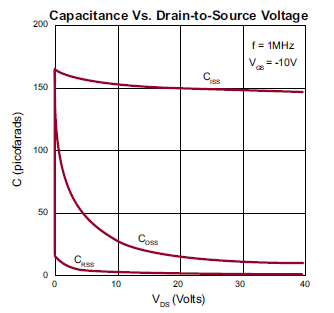
Has anyone any tips on how to model the nonlinear capacitance of MOSFETS? This is the behaviour I'd like to include (of the Supertex DN2530):
Here is the model I've been using for it:
.MODEL DN2530 NMOS (LEVEL=3 RS=0.25 NSUB=5.0E14 DELTA=0.1 KAPPA=0.20 +
TPG=1 CGDO=3.1716E-10 RD=7.0 VTO=-2.20 VMAX=1.0E7 ETA=0.0223089 +
NFS=6.6E10 TOX=750E-10 LD=1.698E-9 UO=862.425 XJ=6.4666E-7 THETA=1.0E-5 +
CGSO=2.50E-9 L=3.0E-6 W=59E-3 KP=12E-6)
Here is the model I've been using for it:
.MODEL DN2530 NMOS (LEVEL=3 RS=0.25 NSUB=5.0E14 DELTA=0.1 KAPPA=0.20 +
TPG=1 CGDO=3.1716E-10 RD=7.0 VTO=-2.20 VMAX=1.0E7 ETA=0.0223089 +
NFS=6.6E10 TOX=750E-10 LD=1.698E-9 UO=862.425 XJ=6.4666E-7 THETA=1.0E-5 +
CGSO=2.50E-9 L=3.0E-6 W=59E-3 KP=12E-6)
As is, it isn't good when comparing a SPICE model against the results of an actual amplifier using the part. On SPICE distortion is pretty low. On the real amp, distortion is relatively high unless driven at the gate from a low impedance or cascoding the device, then it matches SPICE reasonably. Which implies problems with the drain-gate Miller capacitance.
How exactly do you measure capacitance in SPICE? Put a simulated ideal inductor across the terminals and look for where the resonance falls?
How exactly do you measure capacitance in SPICE? Put a simulated ideal inductor across the terminals and look for where the resonance falls?
Probing gate current and voltage should work?How exactly do you measure capacitance in SPICE? Put a simulated ideal inductor across the terminals and look for where the resonance falls?
As is, it isn't good when comparing a SPICE model against the results of an actual amplifier using the part. On SPICE distortion is pretty low. On the real amp, distortion is relatively high unless driven at the gate from a low impedance or cascoding the device, then it matches SPICE reasonably. Which implies problems with the drain-gate Miller capacitance.
How exactly do you measure capacitance in SPICE? Put a simulated ideal inductor across the terminals and look for where the resonance falls?
I realize this starting comment does not directly answer your question, but for good-performing MOSFET amplifiers, the output devices should always be driven by an emitter follower or the like. Amplifiers that drive the lateral or vertical output MOSFETs directly from the VAS are giving up performance at a very small cost savings.
With respect to modeling the capacitances of the MOSFET, I recommend using the VDMOS models with the LTspice simulator. I have some discussion of that in the SPICE modeling chapter in my book.
Notice that the capacitances of the MOSFETs are fairly gentle functions until one gets very close to the rails (e.g., close to clipping). How close to clipping are you running the amplifier when you are making these observations?
Finally, just because SPICE gives lower distortion results than the real-world amplifier is not necessarily the fault of using simulation or having poor models. Without great effort, the SPICE schematic you simulate does not capture all of the real-world nasties, like stray capacitances, stray inductances, nonlineaity from magnetic induction, grounding, etc.
Cheers,
Bob
Thanks, Bob.
The part in question is being used in an input stage (voltage gain with wide drain voltage range, unusual, I know). A somewhat low capacitance part for a high voltage MOSFET, but it does seem to vary a large amount in the first few volts. The data sheet shows the capacitance getting pretty rough when terminal voltage differences get low. I guess that's what you mean by 'close to clipping'? I have found that giving the part more than ten or so volts to work with does drop the measured distortion a lot.
The part in question is being used in an input stage (voltage gain with wide drain voltage range, unusual, I know). A somewhat low capacitance part for a high voltage MOSFET, but it does seem to vary a large amount in the first few volts. The data sheet shows the capacitance getting pretty rough when terminal voltage differences get low. I guess that's what you mean by 'close to clipping'? I have found that giving the part more than ten or so volts to work with does drop the measured distortion a lot.
JLH published a Power Amplifier where the outputs were fed from a higher voltage than that fed to the input stage.Thanks, Bob.
The part in question is being used in an input stage (voltage gain with wide drain voltage range, unusual, I know). A somewhat low capacitance part for a high voltage MOSFET, but it does seem to vary a large amount in the first few volts. The data sheet shows the capacitance getting pretty rough when terminal voltage differences get low. I guess that's what you mean by 'close to clipping'? I have found that giving the part more than ten or so volts to work with does drop the measured distortion a lot.
Many have queried this and suggested that JLH got his numbers swapped around. JLH was maybe making use of higher Vce across the outputs when the input stage was just at the point of clipping.
JLH was very much into combined measurement and subjective sound quality testing.
Has anyone any tips on how to model the nonlinear capacitance of MOSFETS? This is the behaviour I'd like to include (of the Supertex DN2530):
Here is the model I've been using for it:
.MODEL DN2530 NMOS (LEVEL=3 RS=0.25 NSUB=5.0E14 DELTA=0.1 KAPPA=0.20 +
TPG=1 CGDO=3.1716E-10 RD=7.0 VTO=-2.20 VMAX=1.0E7 ETA=0.0223089 +
NFS=6.6E10 TOX=750E-10 LD=1.698E-9 UO=862.425 XJ=6.4666E-7 THETA=1.0E-5 +
CGSO=2.50E-9 L=3.0E-6 W=59E-3 KP=12E-6)
Bill,
I got some of this stuff from Ian Hegglun; he told me sure post it.
So here goes, hope it is helpful.
Jan
Attachments
Here some store still sell 2SK1058 and 2SJ162. I don't know it is fake or not, but some people still love to use them. Sometime I use 10N20 and 10P20 in simulation to replace 2SK1058 and 2SJ162 model from Bob Cordell, but I found they are slightly different on VGS - Id relation.
Here some store still sell 2SK1058 and 2SJ162. I don't know it is fake or not, but some people still love to use them. Sometime I use 10N20 and 10P20 in simulation to replace 2SK1058 and 2SJ162 model from Bob Cordell, but I found they are slightly different on VGS - Id relation.
I haven't heard anyone complain about the sound of the Exicon/Alfet transistors, I've only just seen skepticism. From a technical perspective they are better devices and if they had been available at the time the NECs were king, I think they would have replaced them.
I haven't heard anyone complain about the sound of the Exicon/Alfet transistors, I've only just seen skepticism. From a technical perspective they are better devices and if they had been available at the time the NECs were king, I think they would have replaced them.
I mean, can I use exicon mosfet in simulation but use 2KS1058/SJ162 in real amplifier? I'm worry about biasing the mosfet. But I can accept if the result have higher distortion.
I mean, can I use exicon mosfet in simulation but use 2KS1058/SJ162 in real amplifier? I'm worry about biasing the mosfet. But I can accept if the result have higher distortion.
Don't worry too much about biasing LMOSFETs. To first order, the more bias current the better, as long as things don't get too hot. Given the wide variation among threshold voltages among even the same manufacturer's devices, simulation in regard to bias voltage for a given current may not be of great help anyway - just to first order. There is not really an optimum bias current for MOSFETs for lowest crossover distortion (in contrast to BJTs). I suggest you bias each device at no less than 150mA. I don't remember what bias current Hafler used in the DH200/220. Those amplifiers have two output pair per channel.
Cheers,
Bob

- Home
- Design & Build
- Software Tools
- Better power MOSFET models in LTSpice