Hey All!
First post here, hope I am in the right place/category!
To tip my toes into the world of audio (coming more from the digital design/embedded systems side of things) I wanted to design a relay step attenuator to sit between dac and amp in my schiit stack")
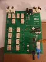
I have gotten the first PCB revision in and the 127 step attenuator works great.
I am however having a little grounding issue.
I have attached the schematic.
In my design the audio path and digital side of things are fully electrically isolated (relays). Audio side is fully passive (ofc) and the digital side of things is powered from a 9v AC mains transformer/adapter.
My setup right now:
(schiit stack is at home, I am stuck at my parent's ... corona...)
My phone (floating ofc) going into the step attenuator powered from the 9vAC adapter, going into my Dad's Violectric HPA V100 ( * grin * )
I am getting a faint but definetly hum through my headphones. That hum goes away completely if I ground my control circuit (for example by plugging in the programmer for the microcontroller, which is grounded through my PC) or by connecting the digital ground to analog ground (which is grounded through the headphone amp)
I was told that most likely i was getting noise coupling through the transformer, which is then coupling through the traces on the PCB.
I am fairly new to analog circuitry so I am a little unsure of what the best move is here. How would I ground the control circuitry? Is there such a thing as a grounded 9Vac adapter? How does a product like the Schiit Stack deal with this (which is also powered by a 9Vac adapter)?
I really would like to stick with the barrel jack if at all possible.
I will have to spin a second revision of the PCB for other reasons, and will pay closer attention to keeping all things seperated but because of enclosour constraints things will have to cross at some point.
Any Ideas?
Thank you all!
Philipp
First post here, hope I am in the right place/category!
To tip my toes into the world of audio (coming more from the digital design/embedded systems side of things) I wanted to design a relay step attenuator to sit between dac and amp in my schiit stack
I have gotten the first PCB revision in and the 127 step attenuator works great.
I am however having a little grounding issue.
I have attached the schematic.
In my design the audio path and digital side of things are fully electrically isolated (relays). Audio side is fully passive (ofc) and the digital side of things is powered from a 9v AC mains transformer/adapter.
My setup right now:
(schiit stack is at home, I am stuck at my parent's ... corona...)
My phone (floating ofc) going into the step attenuator powered from the 9vAC adapter, going into my Dad's Violectric HPA V100 ( * grin * )
I am getting a faint but definetly hum through my headphones. That hum goes away completely if I ground my control circuit (for example by plugging in the programmer for the microcontroller, which is grounded through my PC) or by connecting the digital ground to analog ground (which is grounded through the headphone amp)
I was told that most likely i was getting noise coupling through the transformer, which is then coupling through the traces on the PCB.
I am fairly new to analog circuitry so I am a little unsure of what the best move is here. How would I ground the control circuitry? Is there such a thing as a grounded 9Vac adapter? How does a product like the Schiit Stack deal with this (which is also powered by a 9Vac adapter)?
I really would like to stick with the barrel jack if at all possible.
I will have to spin a second revision of the PCB for other reasons, and will pay closer attention to keeping all things seperated but because of enclosour constraints things will have to cross at some point.
Any Ideas?
Thank you all!
Philipp
Attachments
Having had a read through
Audio Component Grounding and Interconnection
I still am not sure what the best move here is.
If I am going to stick with a 2 pin barrel jack how can I properly ground the circuit? Or do I have to move to another power solution all together?
How does a product like a schiit magni/modi get around this?
Imagine the grounding in actual use with source and amp and actual cabling. If you keep L and R channel GND fully separate internally you are actually creating a ground loop.Is there much benefit in terms of avoiding ground loops by having the l and channels fully seperated? Probably not?
A single DGND to AGND connection at either the input or output side seems like the most sensible option to me here... wherever the lower-impedance earth/ground connection is. If you've got a decent layout with low GND resistance it shouldn't matter much either way, I mean we're talking leakage capacitance of a few hundred pF to mains at most (probably a 3-5 VA transformer tops?), so no super big currents.
Can you post your layout? This appears to be the problem, and can perhaps be fixed with some rerouting. It should be like a board with the power line going to transformer, you want as much distance as possible between the relay circuitry and the switch/signal circuitry, so that the closest they get are at the connections to the relay itself. You could run a ground trace between them (on both sides of the board) as a shield. This still may not eliminate the capacitive coupling between the relay coils and the switches, but should help.
It may be better to connect the grounds, but I'd want that as an option, maybe as a configuration jumper (like on computer boards and hard drives and such), or a switch on the board or on the back of the unit. Likewise, have a switch for the connection below.
On the other hand, connecting L and R grounds together in this unit creates SEVERAL ground loops.Imagine the grounding in actual use with source and amp and actual cabling. If you keep L and R channel GND fully separate internally you are actually creating a ground loop.
It may be better to connect the grounds, but I'd want that as an option, maybe as a configuration jumper (like on computer boards and hard drives and such), or a switch on the board or on the back of the unit. Likewise, have a switch for the connection below.
A single DGND to AGND connection at either the input or output side seems like the most sensible option to me here... wherever the lower-impedance earth/ground connection is. If you've got a decent layout with low GND resistance it shouldn't matter much either way, I mean we're talking leakage capacitance of a few hundred pF to mains at most (probably a 3-5 VA transformer tops?), so no super big currents.
Can you post your layout? ...
... A single DGND to AGND connection at either the input or output side seems like the most sensible option to me here...
Hey All!
Thank you for your help!
I think that jumpers are probably the best move here. Keeps the options open.
Combining L&R Analog ground would only save me 1 physical relay, so the additional cost is not that big. Especially for a hobby project.
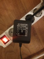
Regarding the transformer: Right now I am using a wall wart transformer rated 9vAC 2000ma. Picture attached.
More about that further down...
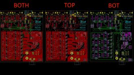
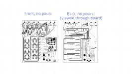
I have attached the PCB layout below, (Images of the front and back layers, plus the whole KiCad Project if that is easier? Not sure what the best format is, let me know if you would prefer something else)
Just wanted to lose a few words about it to explain some of the weirder decisions I made:
My end game here is to fit the whole thing into the enclosure of a Schiit Sys. That is why I went with the transformer.
1) This is definitely not my finest work. It was a test PCB I threw together fairly quickly just to make sure everything worked and I could get the firmware written. The attenuator is OK, but all switching and routing on the top is a mess. I had another order to make and wanted to squeeze it in to save shipping….
2) The two 3.5mm Jacks are mounted on small riser PCBs that sit above the 2x2 pinheader for the external pot. This somewhat weird arrangement is my solution to fitting the 2 3.5mm Jacks, External Poti connection, and Barrel Jack power input in the space between the SYS's RCA jacks.
I wanted all connections on the back, as to not modify the case anywhere else.
3) The formfactor is also the reason for the choice of an external AC adapter. That would make my unit fit with the Magni and Modi I own.
4) This means I am also somewhat stuck with having the Barrel jack power input Right in the middle of my audio IO. The lines will have to cross somewhere. What is the best way to handle this in the final design?
Because I have quite a few parts to fit into not that big of a PCB (with the Switch and Potentiometer placed in such a way as to maximise routing and placement annoyance) I will move to a 4 layer PCB.
I am honestly not sure what the best layout strategy is.
How do I cross the Power line and Signal Lines? at 90 degrees?
How do I handle ground pours if I have 3 different grounds on the same PCB?
My idea at first was to create have a ground pour of the signal ground following both lines around the PCB, as I teste in the attenuator section of the test PCB, mimicking that on the inner layers.
There are a few things I already ran into/realised and will fix in the next revision, just to save you the trouble:
1) The 5V regulator (d-pak) is undersized. I will move to a TH TO-252 with heatsink, maybe even split up the relays on 2 regulators. I could switch to a switch mode, but because I am not really optimizing for cost here I would rather not include such a noise supplying such a small formfactor.
2) Adding pull-downs on the transistor line. While the processor is in start-up/reset, the relays are switching uncontrollably.
3) Polyfuse on the power input, ESD protection on the external potentiometer input. (Would allow me to hook up something like a level pilot to have a nice big control knob on my desk, controlling the internal step attenuator)
4) Screwed up the pinout on the output RCA, fixing that...
Thank you all for the help!
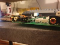
I have attached a shot of the first proto PCB, excuse the messy jumpers fixing my connection mistakes, and the messy programmer connection. I am stuck without my tools at my parent’s place 😊
Attachments
- Status
- This old topic is closed. If you want to reopen this topic, contact a moderator using the "Report Post" button.