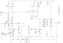
I needed a discrete opamp to replace the one I have in my latest RIAA build so after reading the tech papers regarding the 990 and following the ideas found here: https://www.diyaudio.com/forums/analog-line-level/218373-discrete-opamp-design-173.html#post6071434
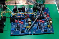
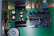
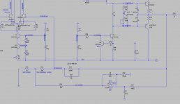
I built the following circuit that am now testing as a line level preamp...
I built the following circuit that am now testing as a line level preamp...
Attachments
Initially I noticed a difficult to null offset,
Unloaded, the response peaked at 250kHz and sinusoids presented distortion in the negative part indicating slew issues.
I reduced IPS current to 4mA (R5 270ohm)
Also reduced VAS current to 9mA (R8 68ohm)
Adjusted output stage idle current to 15mA
Reduced VAS gain by increasing emitter degeneration (R10 57ohm)
And added a capacitor parallel to R10
Now I minimized overshoot and response is flat to 2MHz (unloaded)
Interestingly, the capacitor over R10 must be 330pF when operating at unity gain but it must be higher than 1nF if I use feedback to have gain.
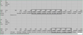
just measured Slew rate:
1kHz 1Vin
Gain = 1.5X (3.5dB) SR 15V/uS
Gain = 3.0X (9.5dB) SR 16V/uS
Gain = 30X (29.5dB) SR 18V/uS
I found that equalizing the currents in the LTP mirror emitter resistors minimizes THD.
That does not mean that the input jfets emitter currents are equal (they are not).
1kHz 1Vin
Gain = 1.5X (3.5dB) SR 15V/uS
Gain = 3.0X (9.5dB) SR 16V/uS
Gain = 30X (29.5dB) SR 18V/uS
I found that equalizing the currents in the LTP mirror emitter resistors minimizes THD.
That does not mean that the input jfets emitter currents are equal (they are not).
In my build I use a trimmer over R1 to null output offset..... now I see this is not the ideal as different values over R1 and R2 will surely increase THD.
My experiments indicate that trimming the input fets degeneration resistors can also null output offset but without affecting THD..... but a trimmer there might leave a strong sonic signature...
My experiments indicate that trimming the input fets degeneration resistors can also null output offset but without affecting THD..... but a trimmer there might leave a strong sonic signature...
Demian Martin suggested:
"This is what I have used very successfully for offset trim. It limits the current through the pot wiper which is important. The resistor in series with the wiper should be adjusted to the largest that will accomodate worst case offset differential between the two fets.
The pot needs to be a good one. I used vishay foil but those are $$$. Carbon would not be good for this. Possibly a wirewound would be the best reasonable but cermet may be as good.
I have also found that a stable thermal housing and reaching operating temperature is important before attempting to adjust.
I have also found that in some cases the lowest distortion is not at the lowest DC offset of the amplifier. usually this is at the -130 dBC distortion levels or lower."
Attachments
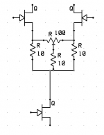
It is interesting to see that the trim current is not injected directly to the inverting input...
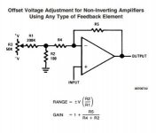
There is some information here EPOT Applications: Offset Adjustment in Op-Amp Circu - Maxim
There is some information here EPOT Applications: Offset Adjustment in Op-Amp Circu - Maxim
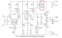
You left out some of the magical components of Deane Jensen's JE-990 design: its mysterious frequency compensation that gives such excellent phase margin. The components you omitted are circled in red below. I've attached the relevant section of Jensen's paper, published in the Journal of the Audio Engineering Society. By the way, if you don't happen to be an AES member, it only costs USD 125 per year, and you get full access to their entire online library of publications.
_
_
Attachments
Thank you Mark
The 990 uses a highish emitter resistor in the VAS... 180ohm... I will read carefully the paper you posted and understand the solutions provided... as I am using a much lower emitter res, I left the zobel out until I totally dominate the technique.
I will try to be a member of AES.
The 990 uses a highish emitter resistor in the VAS... 180ohm... I will read carefully the paper you posted and understand the solutions provided... as I am using a much lower emitter res, I left the zobel out until I totally dominate the technique.
I will try to be a member of AES.
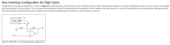
I also found this circuit that might work and I would not need to trim the LTP degeneration resistors:
Regarding this solution, Martin wrote:
"Its a common solution, especially for opamps with no offset trim capability. It does require a stable external supply because the supply is the source of the correction. It can also inject noise etc if its not well managed. The circuit I use is also low noise and independent of external stuff. It would be interesting to check Vgs for a set drain current vs Vds. That has not been an issue in cascoded circuits for me since Vds is essentially fixed. I think internal adjustment of the actual offset would be best, especially if you are starting with closely matched Jfets. BTW I use depletion mode MOSfets for the cascode transistors these days. They work well."
After reading this doc: EPOT Applications: Offset Adjustment in Op-Amp Circu - Maxim
I got an interesting thought...
In the picture of post 8, the nulling offset current is not injected directly into the inverting node, and the reasoning behind is wrote here:
I got an interesting thought...
In the picture of post 8, the nulling offset current is not injected directly into the inverting node, and the reasoning behind is wrote here:
Attachments
Last edited:
I am using a servo to null offset and drift in my DOPA build....
In my opinion if you have to use a DC-servo to null out the DC failure on a discrete opamp someting is very wrong with the design.
I can have a further look at your design, but I don't think that I can't see the whole schema in your pictures.
Stein
Hi stein
In the first post i left a sim with complete circuit.
Hi Ricardo
Thank you, but to see it I have to install LTSpice and that is not going to happen.
I have looked on some of your previous posts and can see your "design".
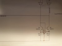
I think you should try a 10k pot. with the wiper connected at the positive rail and the element between R1 and R2 see the drawing, that should null the DC offset at the output.
(This i my opinion: I would not null the offset like Damian is suggesting and in case you intend to use a DC servo I would not connect it to the negative input.)
One question why do you select this design and what is the reason you have chosed to use JFET ips instead of BJT?
In my opinion, if you for some reasons prefere JFET ips instead of BJT there are much better ways to design a circuit with lower noise and THD that will fit into a 990 package.
Stein
Attachments
Last edited:
- Status
- This old topic is closed. If you want to reopen this topic, contact a moderator using the "Report Post" button.
- Home
- Source & Line
- Analog Line Level
- Discrete opamp offset trim