Kazuo Ozawa and Bunpei are collaborating in a new application of GaN transistor as a replacement of SiC rectifiers for power supplies used in digital audio devices. They think this is a novel approach and worth sharing on this forum.
For these years, Kazuo has made his efforts mainly on improving Salas Reflektor type and Taylor Follower type regulators. Recently, he applied GaN transistor, GS66502B of GaN Systems as a replacement of SiC MOSFET, C3M0280090 of CREE and obtained a satisfactory result.
http://john.asablo.jp/blog/img/2016/12/19/458cae.png
http://john.asablo.jp/blog/img/2017/01/17/460d69.jpg
On the other hand, Bunpei has tried such SiC rectifiers as manufactured by CREE, Rohm, Infineon. His latest favor was Infineon G6. He read Kazuo's blog post and thought, "Is there any GaN rectifier? That must be interesting."
There was a hint on a technical presentation given by Sanghyeon Park and Juan Rivas-Davila.
https://superlab.stanford.edu/poster/APEC2017_slides_Sanghyeon.pdf
They said, "Tying the gate to the source makes GaN transistor behave like a diode.". Bunpei's first attempt was not successful because the GaN transistor got very hot in his environment. He asked Kazuo to apply GS66502B with his custom board especially designed for cooling.
At the beginning of this month, Kazuo reported his first result on his blog page in Japanese,
GaN Transistorをダイオードとして使う: Konちゃんの虫眼鏡
expressing his very good comments on the new rectifiers. He applied the GaN transistors in PSU of full-wave rectification for an OCXO master clock generator.
Bunpei immediately purchased GS61008T, which has a thermal pad on its top , and followed Kazuo's approach. Bunpei applied the rectifiers to PSU of full-wave rectification with both 4 diodes type and 2 diodes type. Those PSUs are used for Chiaki's SDTrans384 SD memory card transport, ES9038PRO Dual Mono DAC and NDK DuCULoN OCXO master clock generator.
Bunpei's impressions for the new GaN rectifiers were very similar to those given by Kazuo. Both of them felt something very new and remarkable in the improvement of resultant sound quality. "It's a kind of quantum leap!"
Kazuo and Bunpei hope that DIY audiophiles on this forum will confirm their claim is not any bluff and will have a happy music.
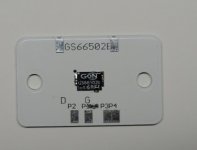
You can easily purchase those GaN transistors, products of GaN Systems via Mouser. For cooling, Kazuo designed a special circuit board and Bunpei soldered a small piece of copper plate on the thermal pad of the GaN chip.
For these years, Kazuo has made his efforts mainly on improving Salas Reflektor type and Taylor Follower type regulators. Recently, he applied GaN transistor, GS66502B of GaN Systems as a replacement of SiC MOSFET, C3M0280090 of CREE and obtained a satisfactory result.
http://john.asablo.jp/blog/img/2016/12/19/458cae.png
http://john.asablo.jp/blog/img/2017/01/17/460d69.jpg
On the other hand, Bunpei has tried such SiC rectifiers as manufactured by CREE, Rohm, Infineon. His latest favor was Infineon G6. He read Kazuo's blog post and thought, "Is there any GaN rectifier? That must be interesting."
There was a hint on a technical presentation given by Sanghyeon Park and Juan Rivas-Davila.
https://superlab.stanford.edu/poster/APEC2017_slides_Sanghyeon.pdf
They said, "Tying the gate to the source makes GaN transistor behave like a diode.". Bunpei's first attempt was not successful because the GaN transistor got very hot in his environment. He asked Kazuo to apply GS66502B with his custom board especially designed for cooling.
At the beginning of this month, Kazuo reported his first result on his blog page in Japanese,
GaN Transistorをダイオードとして使う: Konちゃんの虫眼鏡
expressing his very good comments on the new rectifiers. He applied the GaN transistors in PSU of full-wave rectification for an OCXO master clock generator.
Bunpei immediately purchased GS61008T, which has a thermal pad on its top , and followed Kazuo's approach. Bunpei applied the rectifiers to PSU of full-wave rectification with both 4 diodes type and 2 diodes type. Those PSUs are used for Chiaki's SDTrans384 SD memory card transport, ES9038PRO Dual Mono DAC and NDK DuCULoN OCXO master clock generator.
Bunpei's impressions for the new GaN rectifiers were very similar to those given by Kazuo. Both of them felt something very new and remarkable in the improvement of resultant sound quality. "It's a kind of quantum leap!"
Kazuo and Bunpei hope that DIY audiophiles on this forum will confirm their claim is not any bluff and will have a happy music.
You can easily purchase those GaN transistors, products of GaN Systems via Mouser. For cooling, Kazuo designed a special circuit board and Bunpei soldered a small piece of copper plate on the thermal pad of the GaN chip.
It is a bit hard to decipher what they think is going on...
Language similar to the above is not very helpful... Then again I am probably not in a position to comment.
Otherwise let's all race out and buy these things to try them out.
https://www.mouser.com/ds/2/692/GS61008T DS Rev 160319-913415.pdf
https://www.wolfspeed.com/media/downloads/825/C3M0280090D.pdf
Data Sheet for the GS61008T indicates 0 reverse recovered charge implying no minority carriers in the device.
Accordingly there is no quoted reverse recovery time, Trr. However device capacitance and their associated charges still exists. Otherwise the device appears to not have a parasitic Body Source diode.
Data Sheet for the C3M0280090D quotes figures for recovered charge and therefore includes figures for reverse recovery time. This is in addition to device capacitances and their associated charges under given conditions. The device does have a parasitic Body Source diode.
https://superlab.stanford.edu/poster/APEC2017_slides_Sanghyeon.pdf
Amongst other repetitive things the Author seems to be having problems with Simulation not matching Reality in respect of power losses. A wet finger may suggest that the model is inaccurate... everyone moans about simulation in respect of such anomalies.
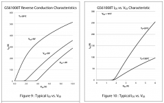
Picture from the GS61008T data sheet attached.
It might be pertinent from the right side graph of Ids vs Vgs that the 'channel' does not become conductive until Vgs hits about 2V.
Looking at the left side graph of Isd vs Vsd the Vgs = 0V curve only begins to show conduction as Vds rises to 2V. The Vgs = -2V only begins to show conduction as Vds rises to 4V. The same offset.
This is the forward conduction drop of the equivalent diode but it is not a diode...
This might be the reason why simulation does not follow reality. Does the model include such effects?
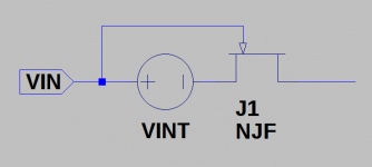
Going off the wall if you tie gate to source and then reverse bias the device what happens internally when it is conducting in the reverse mode?
Second Picture is a poor representation of what might be happening internally.
VINT is a voltage drop across the internal Source with the Gate tied to the package source. With Zero volts external the internal drop is negative with respect to the Gate and.... the device turns on.
The above might be rubbish but in terms of how it sounds...
Are Schottky diodes, majority carrier devices sonically as good as the above proposal?
Perhaps Bunpei can try them out and report back.
Bunpei's impressions for the new GaN rectifiers were very similar to those given by Kazuo. Both of them felt something very new and remarkable in the improvement of resultant sound quality. "It's a kind of quantum leap!"
Kazuo and Bunpei hope that DIY audiophiles on this forum will confirm their claim is not any bluff and will have a happy music.
Language similar to the above is not very helpful... Then again I am probably not in a position to comment.
Otherwise let's all race out and buy these things to try them out.
https://www.mouser.com/ds/2/692/GS61008T DS Rev 160319-913415.pdf
https://www.wolfspeed.com/media/downloads/825/C3M0280090D.pdf
Data Sheet for the GS61008T indicates 0 reverse recovered charge implying no minority carriers in the device.
Accordingly there is no quoted reverse recovery time, Trr. However device capacitance and their associated charges still exists. Otherwise the device appears to not have a parasitic Body Source diode.
Data Sheet for the C3M0280090D quotes figures for recovered charge and therefore includes figures for reverse recovery time. This is in addition to device capacitances and their associated charges under given conditions. The device does have a parasitic Body Source diode.
https://superlab.stanford.edu/poster/APEC2017_slides_Sanghyeon.pdf
Amongst other repetitive things the Author seems to be having problems with Simulation not matching Reality in respect of power losses. A wet finger may suggest that the model is inaccurate... everyone moans about simulation in respect of such anomalies.
Picture from the GS61008T data sheet attached.
It might be pertinent from the right side graph of Ids vs Vgs that the 'channel' does not become conductive until Vgs hits about 2V.
Looking at the left side graph of Isd vs Vsd the Vgs = 0V curve only begins to show conduction as Vds rises to 2V. The Vgs = -2V only begins to show conduction as Vds rises to 4V. The same offset.
This is the forward conduction drop of the equivalent diode but it is not a diode...
This might be the reason why simulation does not follow reality. Does the model include such effects?
Going off the wall if you tie gate to source and then reverse bias the device what happens internally when it is conducting in the reverse mode?
Second Picture is a poor representation of what might be happening internally.
VINT is a voltage drop across the internal Source with the Gate tied to the package source. With Zero volts external the internal drop is negative with respect to the Gate and.... the device turns on.
The above might be rubbish but in terms of how it sounds...
Are Schottky diodes, majority carrier devices sonically as good as the above proposal?
Perhaps Bunpei can try them out and report back.
Attachments
Hi, MorbidFractal!
I appreciated your comments very much!
This explanation might be helpful.
"Does the GaN enhancement mode HEMT have a body diode? How do the reverse conduction characterisitcs compare with Sillicon MOSFET?"
GaN FAQs | GaN Systems
Bunpei
I appreciated your comments very much!
Going off the wall if you tie gate to source and then reverse bias the device what happens internally when it is conducting in the reverse mode?
This explanation might be helpful.
"Does the GaN enhancement mode HEMT have a body diode? How do the reverse conduction characterisitcs compare with Sillicon MOSFET?"
GaN FAQs | GaN Systems
Bunpei
At Mouser, an unit price of GS61008T for Qty. 1 is USD 7.60. It is not cheap. I think worth paying, however.
Not bad, usually RF HEMTs are around 60-100 USD, 7.60 is not bad at all.
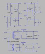
As Bunpei precisely reports, my first interest for GaN started from the study of Taylor Follower type Regulator. When I replaced MTP3055VL with GS66502B for
shunt on the regulator, I found great improvement. Then I decided to apply this GaN to Power amplifier particularly the Amazing Circlotron.
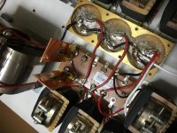
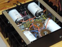
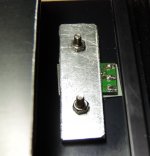
In reference to Amazing Circlotron I made one modification which is adding cascode to the first stage. (1st picture)
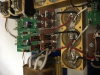
On 2nd picture shows you how to implement GaN on a heat sink, Gan is beneath a small aluminum panel.
Also, you can see the modified Amazing Circlotron which I made on 3rd picture.
The sound of this amp made excites me. I used to use some bipolar transistors, MOSFETs, and tubes for final stage until then, I guess GaN is best of all and have no need to choose other items anymore IMO.
There are two challenges.
First one is the green board of GaN is too small to satisfy maximum consumption of heat. Then I made the board made of aluminum substrate (4th picture).
The second one is to change rectifiers to GaNs which I use Infineon G5 SiC diodes now.
Until this late spring, I will report next modified amp with GaN.
shunt on the regulator, I found great improvement. Then I decided to apply this GaN to Power amplifier particularly the Amazing Circlotron.
In reference to Amazing Circlotron I made one modification which is adding cascode to the first stage. (1st picture)
On 2nd picture shows you how to implement GaN on a heat sink, Gan is beneath a small aluminum panel.
Also, you can see the modified Amazing Circlotron which I made on 3rd picture.
The sound of this amp made excites me. I used to use some bipolar transistors, MOSFETs, and tubes for final stage until then, I guess GaN is best of all and have no need to choose other items anymore IMO.
There are two challenges.
First one is the green board of GaN is too small to satisfy maximum consumption of heat. Then I made the board made of aluminum substrate (4th picture).
The second one is to change rectifiers to GaNs which I use Infineon G5 SiC diodes now.
Until this late spring, I will report next modified amp with GaN.
Attachments
As Bunpei precisely reports, my first interest for GaN started from the study of Taylor Follower type Regulator. When I replaced MTP3055VL with GS66502B for
shunt on the regulator, I found great improvement. Then I decided to apply this GaN to Power amplifier particularly the Amazing Circlotron.
In reference to Amazing Circlotron I made one modification which is adding cascode to the first stage. (1st picture)
On 2nd picture shows you how to implement GaN on a heat sink, Gan is beneath a small aluminum panel.
Also, you can see the modified Amazing Circlotron which I made on 3rd picture.
The sound of this amp made excites me. I used to use some bipolar transistors, MOSFETs, and tubes for final stage until then, I guess GaN is best of all and have no need to choose other items anymore IMO.
Dear Kazuo Ozawa,
Do you think GaN mosfet can apply on preamplifier?
For example to replace 2SK214/2SK215/2SK216 ?
I am afraid I can't answer your question properly.
I have adopted 2SK214 a few years ago on my Power amp, the performance is good.
For the answer would depend on the topology of preamplifier that you plan, I can't say yes or no.
But I also imagine to apply GaN on 1st stage of Power amp or line amp of DAC, and guess that it may be easy to accomplish.
Thanks.
I am afraid I can't answer your question properly.
I have adopted 2SK214 a few years ago on my Power amp, the performance is good.
For the answer would depend on the topology of preamplifier that you plan, I can't say yes or no.
But I also imagine to apply GaN on 1st stage of Power amp or line amp of DAC, and guess that it may be easy to accomplish.
Thanks.
I have seem many preamplifier using 2SK214/2SJ76 as output stage.
So, if Gan is a good choice, I may apply it to replace 2SK214 at preamplifier stage.
I have seem many preamplifier using 2SK214/2SJ76 as output stage.
So, if Gan is a good choice, I may apply it to replace 2SK214 at preamplifier stage.
That sounds good.
But there is no p-ch GaN, how do you replace 2SJ76?
That sounds good.
But there is no p-ch GaN, how do you replace 2SJ76?
One of my preamplifier are using two pcs of 2SK214(no need 2SJ76) at output stage. The idea is came from Japan MJ magazine master. His design is using same type of FET or MOSFET on every stage. For example 1 stage is N type FET, 2nd stage is P type FET, 3rd stage is N tpe MOSFET.
LT4320+GS61008T: Ideal Diode Bridge Approach
The GaN E mode transistor, GS61008T is a normally-OFF type.
Some of you may remember an "Ideal Diode Bridge" and a driver IC for that purpose.
A Japanese blogger of this page (in Japanese),
LT4320+GS61008T(GaN)_LTspice: アナログ回路のおもちゃ箱
kindly performed a LTspice simulation for a combination of LT4320 and GS61008T, presenting such a result that;
"LT4320 is supposed to be able to drive GS61008T."
I think we can expect a better efficiency by using this configuration.
Great one. I have done the same simulation in LTSpice before I see this article and should work fine, with much less heat generated against using GaN transistors as diode by binding G and S.
Ordered some GS61008T from Mouser and will test later.
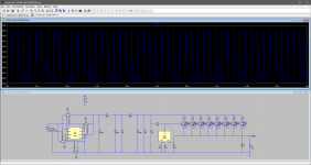
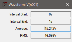
GaN FET full wave rectifier for 13D2 line amplifier by Kazuo
On Kazuo's blog page (in Japanese language), he posted a new application of GaN FET full wave rectifier to PSU for his 13D2 line amplifier.
13D2ラインアンプにGaNを投入する: Konちゃんの虫眼鏡
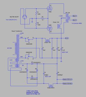
His GaN FET is GaN Systems GS6502B and his configuration is of body diode, tying G and S.
He reports the same kind of significant SQ improvement that he perceived in his previous application to PSU for OCXO master clock generator. Bunpei thinks his impression is also similar to Bunpei's.
On Kazuo's blog page (in Japanese language), he posted a new application of GaN FET full wave rectifier to PSU for his 13D2 line amplifier.
13D2ラインアンプにGaNを投入する: Konちゃんの虫眼鏡
His GaN FET is GaN Systems GS6502B and his configuration is of body diode, tying G and S.
He reports the same kind of significant SQ improvement that he perceived in his previous application to PSU for OCXO master clock generator. Bunpei thinks his impression is also similar to Bunpei's.
- Status
- This old topic is closed. If you want to reopen this topic, contact a moderator using the "Report Post" button.
- Home
- Amplifiers
- Power Supplies
- Applying GaN transistor as a replacement of SiC rectifier