Hi to all
i try to measure my HArman Kardon HS500 class D amp (DDX 2160 chip). first try
my envoirment:
dummy load about 4ohms load each channel (mounted on an old cdp chassis-fan will be updated)
input is over rigol with 1kHz and 0,775 Vpp to aux in of the HS500 amp
right channel is with an ampere meter to check the current.
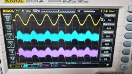
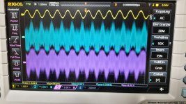
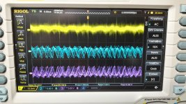
scope: yellow channel 1 is input (auxin),blue is right channel, and purple is left channel
on the very right side you will see the probes af a 2nd DMM, but this just check the volts at the amp board (is really stable at 34,55- 34,65Vdc!!!)
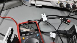
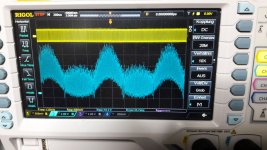
pic 1 (left to right) shows the scope probes : auxin yellow, blue and purple R + L channel
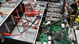
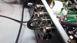
pic 2 the DUT right and the dummy load (4ohms 100WATT each channel ) on the left, scope probes are connected on the housing of the AMP (GND) the HS500 has no earth connection.
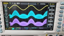
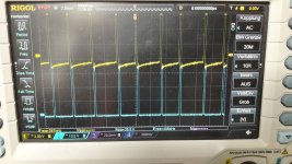
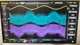
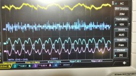
pic 3 is half volume all channels
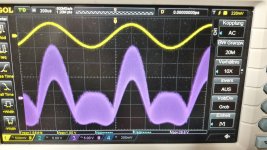
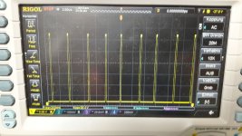
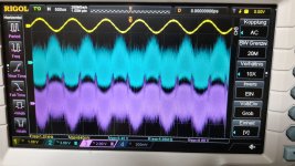
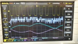
pic 4 is full power at 1khz just switch the channel R off to see more
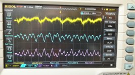
pic 5 is the check of ocp - with the ampere meter on channel R
as you can see i try to see some output (and first time power measurments). So why i get so strange output signals? the form looks distroyed.
did i something wrong?
thx for your inputs...
i try to measure my HArman Kardon HS500 class D amp (DDX 2160 chip). first try
my envoirment:
dummy load about 4ohms load each channel (mounted on an old cdp chassis-fan will be updated)
input is over rigol with 1kHz and 0,775 Vpp to aux in of the HS500 amp
right channel is with an ampere meter to check the current.
scope: yellow channel 1 is input (auxin),blue is right channel, and purple is left channel
on the very right side you will see the probes af a 2nd DMM, but this just check the volts at the amp board (is really stable at 34,55- 34,65Vdc!!!)
pic 1 (left to right) shows the scope probes : auxin yellow, blue and purple R + L channel
pic 2 the DUT right and the dummy load (4ohms 100WATT each channel ) on the left, scope probes are connected on the housing of the AMP (GND) the HS500 has no earth connection.
pic 3 is half volume all channels
pic 4 is full power at 1khz just switch the channel R off to see more
pic 5 is the check of ocp - with the ampere meter on channel R
as you can see i try to see some output (and first time power measurments). So why i get so strange output signals? the form looks distroyed.
did i something wrong?
thx for your inputs...
Attachments
Last edited:
hi
is there a problem with the appr. 4 ohms load? but the signal is at low volume still "distroyed". (first pic = pic 1 )
beacuse of my last days illness a did no furhter tests. i try to push the amp with different frequ to see the ocp.....yes you can hear a "queeeek" and the current goes down....but its another thing...
datasheets : DDX 2160 and DDX 8001 are uploaded...
any ideas?
is there a problem with the appr. 4 ohms load? but the signal is at low volume still "distroyed". (first pic = pic 1 )
beacuse of my last days illness a did no furhter tests. i try to push the amp with different frequ to see the ocp.....yes you can hear a "queeeek" and the current goes down
....but its another thing...datasheets : DDX 2160 and DDX 8001 are uploaded...
any ideas?
Attachments
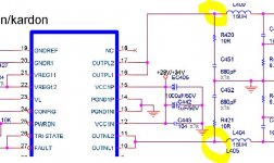
The modulator IC and output stage ICs are fully digital, with digital inputs only. The signal does not adopt an analog representation at any point in the modulator or output stage, until after the LC output filters.
The output signal shows a defect (bottom half missing, still switching) that does not match with a digital problem.
In my opinion the problem is analog (negative low voltage rail missing, or broken IC), and it is located in the circuits that condition analog input signal and turn it to digital. A digital sound source, if supported, skipping analog input, could help to diagnose this.
The modulator IC and output stage ICs are fully digital, with digital inputs only. The signal does not adopt an analog representation at any point in the modulator or output stage, until after the LC output filters.
The output signal shows a defect (bottom half missing, still switching) that does not match with a digital problem.
In my opinion the problem is analog (negative low voltage rail missing, or broken IC), and it is located in the circuits that condition analog input signal and turn it to digital. A digital sound source, if supported, skipping analog input, could help to diagnose this.
Thank you Eva, thanks that you take time to go through that
 .....thanks a lot.
yesterday i checked additionally the load with 8Ohms but as expected -- same result.
according to the pcb lines the stereo is not done by 1 chip only...so that means 2 chip broken?....i guess no....... it must be something before.. i will try with digital in
Last edited:
good evening
i go ahead with measruments. digital in. i did this with an DVD player and a test CD with 1khz test tone. via digital wyde eye cable to the amps coax input.
pic 1 shows the result..the same result...so i guess the chip is gone..
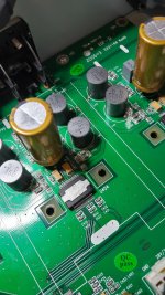
pic 2 i put the heatsinks off - to have better way for measuremnts. the chip is over 8 ohm resitor load getting hot 60°C. after 5 mins.
pic 3 +4 i measure directly on the Resistors which are connected to the outputs of the chip before the L
...... directly on the ddx2160 pins is not possible....i am afraid to make shorts....its too small
pic 3 and 4 looks like a PWM (before the L ...then to the LS outputs)
Q1 is it possible that i shoot the chip after to heavy load tests? i did several time the ocp tests.
i go ahead with measruments. digital in. i did this with an DVD player and a test CD with 1khz test tone. via digital wyde eye cable to the amps coax input.
pic 1 shows the result
..the same result...so i guess the chip is gone..pic 2 i put the heatsinks off - to have better way for measuremnts. the chip is over 8 ohm resitor load getting hot 60°C. after 5 mins.
pic 3 +4 i measure directly on the Resistors which are connected to the outputs of the chip before the L
...... directly on the ddx2160 pins is not possible....i am afraid to make shorts....its too small
pic 3 and 4 looks like a PWM (before the L ...then to the LS outputs)
Q1 is it possible that i shoot the chip after to heavy load tests? i did several time the ocp tests.
Attachments
I forgot to mention this in previous post: Remember this is class BD full bridge, always bridged, one output lead does the positive half of the wave, the other does the negative half. In order to measure output signal, some system for sensing speaker +OUT and -OUT differentially is needed. The proper signal won't be obtained by grounding a single ended oscilloscope probe to GND and connecting tip to +OUT. At least 2 probes are required, one for +OUT and one for -OUT, and the waves have to be displayed in sync (-OUT with inverted phase) to observe the effect. I do not recommend grounding the oscilloscope to an active class-D speaker output, at least not without a CM choke and lifting the ground of oscilloscope power cord, also no data cable allowed to oscilloscope, if any.
Last edited:
Hi
i did the measurment as "requested"
pic 1 -3 are
yellow channel 1 AUXIN (1kHz 0,775Vpp) to the amp
8 ohms dummy load each channel
blue -channel 2 = Rchannel + plus
purple - channel 3 = R-channel - minus (is inverted)
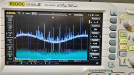
pic 4-5 are the try to show the math A+B (channel 2+3)
i moved the channel 2 +3 down so that on the disply more of the daark blue (math) is visible
Is this math correct? lot of spikes! What are these?
Can I see the distrotions of the BD switching of both halfs?
thnaks for you time and help
i did the measurment as "requested"
pic 1 -3 are
yellow channel 1 AUXIN (1kHz 0,775Vpp) to the amp
8 ohms dummy load each channel
blue -channel 2 = Rchannel + plus
purple - channel 3 = R-channel - minus (is inverted)
pic 4-5 are the try to show the math A+B (channel 2+3)
i moved the channel 2 +3 down so that on the disply more of the daark blue (math) is visible
Is this math correct? lot of spikes! What are these?
Can I see the distrotions of the BD switching of both halfs?
thnaks for you time and help
Attachments
Last edited:
I forgot to mention this in previous post: Remember this is class BD full bridge, always bridged, one output lead does the positive half of the wave, the other does the negative half. In order to measure output signal, some system for sensing speaker +OUT and -OUT differentially is needed. The proper signal won't be obtained by grounding a single ended oscilloscope probe to GND and connecting tip to +OUT. At least 2 probes are required, one for +OUT and one for -OUT, and the waves have to be displayed in sync (-OUT with inverted phase) to observe the effect. I do not recommend grounding the oscilloscope to an active class-D speaker output, at least not without a CM choke and lifting the ground of oscilloscope power cord, also no data cable allowed to oscilloscope, if any.
sorry.... i go trough agian.
Question1
So no GND Probe of the scope to chassis of the amp?
and the waves have to be displayed in sync (-OUT with inverted phase
Q2
Channel for Out- has to be synch of Channel Out+? How can i do that?
thx
Speaker OUT- is not amplifier ground.
Additionally, chassis ground is not always amplifier ground.
I mean two probes grounded to amplifier ground, to monitor both active outputs.
To find out if the traces are already in sync in the display, or need to be synchronized, check oscilloscope manual.
Grounding a probe to OUT- is the complex thing, as oscilloscope ground becomes no longer ground during the measurement. Additional complexity is due to the fact that there is HF carrier residual in output terminals.
I think you did it right in the pictures of previous post, although display is quite fuzzy, as it is when too much data is averaged (too low frequency, too wide span), and when the signal being measured is not higher in amplitude that carrier residual.
To see more audio and less carrier a pair of RC lowpass filters can be used.
Summing is only good at audio frequencies, not good at HF, because the modulation is not synchronized with test signal or between channels.
Last edited:
Speaker OUT- is not amplifier ground.
thx...i know...a scope is not a multimeter
Additionally, chassis ground is not always amplifier ground.
I mean two probes grounded to amplifier ground, to monitor both active outputs.
i checked the GND points to chassis with my R-meter.
but....
this is a topic which let me get crazy. on all pcb the GND is connected to the metal chassis - but the chassis is not connected with the earth to AC earth! the housing is metal. so how is this amp getting the "certification" in EU ???
maybe i am to old to understand this...
To find out if the traces are already in sync in the display, or need to be synchronized, check oscilloscope manual.
Grounding a probe to OUT- is the complex thing, as oscilloscope ground becomes no longer ground during the measurement. Additional complexity is due to the fact that there is HF carrier residual in output terminals.
....äääähmmm...i agree....
I think you did it right in the pictures of previous post,
although display is quite fuzzy, as it is when too much data is averaged (too low frequency, too wide span), and when the signal being measured is not higher in amplitude that carrier residual.
To see more audio and less carrier a pair of RC lowpass filters can be used.
Summing is only good at audio frequencies, not good at HF, because the modulation is not synchronized with test signal or between channels.
again . thanks Eva for your time to help me
Last edited:
but....
this is a topic which let me get crazy. on all pcb the GND is connected to the metal chassis - but the chassis is not connected with the earth to AC earth! the housing is metal. so how is this amp getting the "certification" in EU ???
maybe i am to old to understand this...
i correct myself:
the protection is done by additionally Plactic cover under all PCB to the ground plate of the chassis...so its according to the norm.
so check all old devices if this is implemented and the extra plastic cover is ok.
noise measurement...
Hi again
i want to go ahead with my amp measurments. please give me feedback if my things are nonsense...thanks
case 1
the noise if i shortcut the aux in.
input = aux in = is yellow channel 1
blue is out+ channel 2
purple is out - (inverted) channel 3
pic 1 is a single shot with the scope, pic 2 is the same with run modus on the sscope. nice to see the BTL mode...1 half of each of the OUT
pic 3 is how i do the short...i compare it with a rca connector...its the same mearuement.
case 2
next is the coax in (not shorted)in yellow = channel 1
blue is out+ channel 2
purple is out - (inverted) channel 3
pic 4 and 5 are the measurments with the try to do the math function as discribed in one of my previous posts.nice to see the BTL mode...1 half of each of the OUT
in both cases the output is about 1 Volt.
for aux in i made no pic...
it is not changing if i push the volume at max. the only thing that on a 4 ohm loudspeaker i can hear nothing.
normal?
good night and thanks for your time to help me.....
Hi againi want to go ahead with my amp measurments. please give me feedback if my things are nonsense.
..thankscase 1
the noise if i shortcut the aux in.
input = aux in = is yellow channel 1
blue is out+ channel 2
purple is out - (inverted) channel 3
pic 1 is a single shot with the scope, pic 2 is the same with run modus on the sscope. nice to see the BTL mode...1 half of each of the OUT
pic 3 is how i do the short...i compare it with a rca connector...its the same mearuement.
case 2
next is the coax in (not shorted)in yellow = channel 1
blue is out+ channel 2
purple is out - (inverted) channel 3
pic 4 and 5 are the measurments with the try to do the math function as discribed in one of my previous posts.nice to see the BTL mode...1 half of each of the OUT
in both cases the output is about 1 Volt.
for aux in i made no pic...
it is not changing if i push the volume at max. the only thing that on a 4 ohm loudspeaker i can hear nothing.
normal?
good night and thanks for your time to help me.....
Attachments
Last edited:
This is "digital clocked class BD BTL modulation".
- The PWM pulse width comes in N*clock increments.
- The exact pulse width needed does not exist, so in absence of signal the system can be observed alternating between pulses of length N and N+1, at a rate such that the average is the pulse width required.
- The PWM-to-voltage gain of a LC filter is only constant when inductor current is not allowed to fall and stay at zero, so the circuit keeps producing alternate positive and negative pulses when idle, to keep inductor current away from zero.
- This is noisier than class AD, but at just 20V to 30V maximum amplitude of signal that can be put into the speakers by the circuit, and considering that the speakers used with these receivers are almost always under 90dB/W sensitivity, a 100dB SNR (quoted for DDX-8001) is low enough to result in idle noise floor inaudible in normal usage conditions.
In comparison, SNR requirements are more severe for higher power amplifiers producing 3~6 times more voltage (10~16dB), for professional usage, where speaker sensitivity can be as high as 100dB/W. In this case 120dB SNR are needed for the same perceived result. This is my field of work.
The HK chipset is designed to be used in amplifiers of moderate power output, and to achieve low power cunsumption when idle. The open-loop principle is designed to allow producing multi-channel amplifiers with as much automated assembly and off-the-shelf parts as possible, and with as few parts as possible, apart from the custom chips. This is done from the point of view that expense in more complex silicon pays for savings in assembly cost. This is not always true, chips have to be somewhat standard in function and interface to stay selling for long, to pay back R&D.
Of course they are failing consistence somewhere. The power supply is neither conceived nor produced by the same people, it does not follow same design principles. The pictures reveal it is the design style from oriental (China, Taiwan, Korea) SMPS engineers, with many transformers for something that can be done with less, magnetics wound semi-automatically in far-East factories with thousands of workers, single sided huge PCB, thru-hole parts, with some types of components often inserted manually (again in far-East factories with thousands of workers).
Last edited:
This is "digital clocked class BD BTL modulation".
- .......
- The PWM-to-voltage gain of a LC filter is only constant when inductor current is not allowed to fall and stay at zero, so the circuit keeps producing alternate positive and negative pulses when idle, to keep inductor current away from zero.
-s).
sorry that brings me back to my level..---> i am a noob
any nice link to read through that?
- Status
- This old topic is closed. If you want to reopen this topic, contact a moderator using the "Report Post" button.
- Home
- Amplifiers
- Class D
- HK HS500 - power and other measurements