Hey guys I'm trying to repair a faulty KEF HTB2 subwoofer that happens to revolve around a 200ASC module from B&O.
The faults lie within the power supply section and during the initial failure a chain reaction of destruction occurred where several components failed. The problem here is that upon failing any markings that would otherwise identify said components ended up either charred black or in pieces.
I have scrounged the internet high and low for detailed images of the power section but haven't been able to find very much. A few images here and there, useful as a starting point, but not really enough.
The version that I've got is revision F.
Schematics for this are unobtanium, so if anyone could take some detailed pictures of the power section that would be most appreciated.
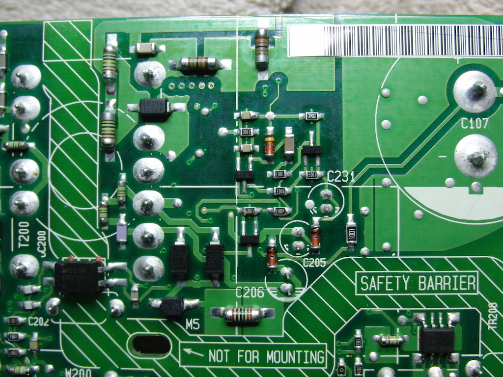
What I'm after are the resistor values for the components surrounding the main SMPS controller, I think this is an NPC1203D6, but that was from an image taken of a different revision. Resistor values for both the top side and bottom side are necessary as the destruction spread wide and far!
So far I've replaced the dead transistors, power MOSFET, controller, aux protection zeners and some resistors with what I could make out but no luck. The device fails to start-up and when the aux supply is provided externally it will start (and then continue working when the external supply is removed) but no regulation occurs.
The faults lie within the power supply section and during the initial failure a chain reaction of destruction occurred where several components failed. The problem here is that upon failing any markings that would otherwise identify said components ended up either charred black or in pieces.
I have scrounged the internet high and low for detailed images of the power section but haven't been able to find very much. A few images here and there, useful as a starting point, but not really enough.
The version that I've got is revision F.
Schematics for this are unobtanium, so if anyone could take some detailed pictures of the power section that would be most appreciated.
What I'm after are the resistor values for the components surrounding the main SMPS controller, I think this is an NPC1203D6, but that was from an image taken of a different revision. Resistor values for both the top side and bottom side are necessary as the destruction spread wide and far!
So far I've replaced the dead transistors, power MOSFET, controller, aux protection zeners and some resistors with what I could make out but no luck. The device fails to start-up and when the aux supply is provided externally it will start (and then continue working when the external supply is removed) but no regulation occurs.
May be worth trying http://www.diyaudio.com/forums/members/ghentxu.html @ Ghent Audio - he seems to cover most things IcePower...
Interesting, what version is it that you've got because there are subtle differences between what you've got and what I'm working with!
The feedback from the optocoupler circuit is slightly simpler. As a last resort I've been thinking about remaking a small PCB just for the controller and simplifying the entire circuit surrounding it. B&Os seems unnecessarily complex compared to the application notes for the part. Whatever reason they had for adding all the extra parts it certainly didn't protect the thing from exploding.
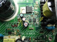
I've taken your photos and added stuff to them to show what it is I need and a question")
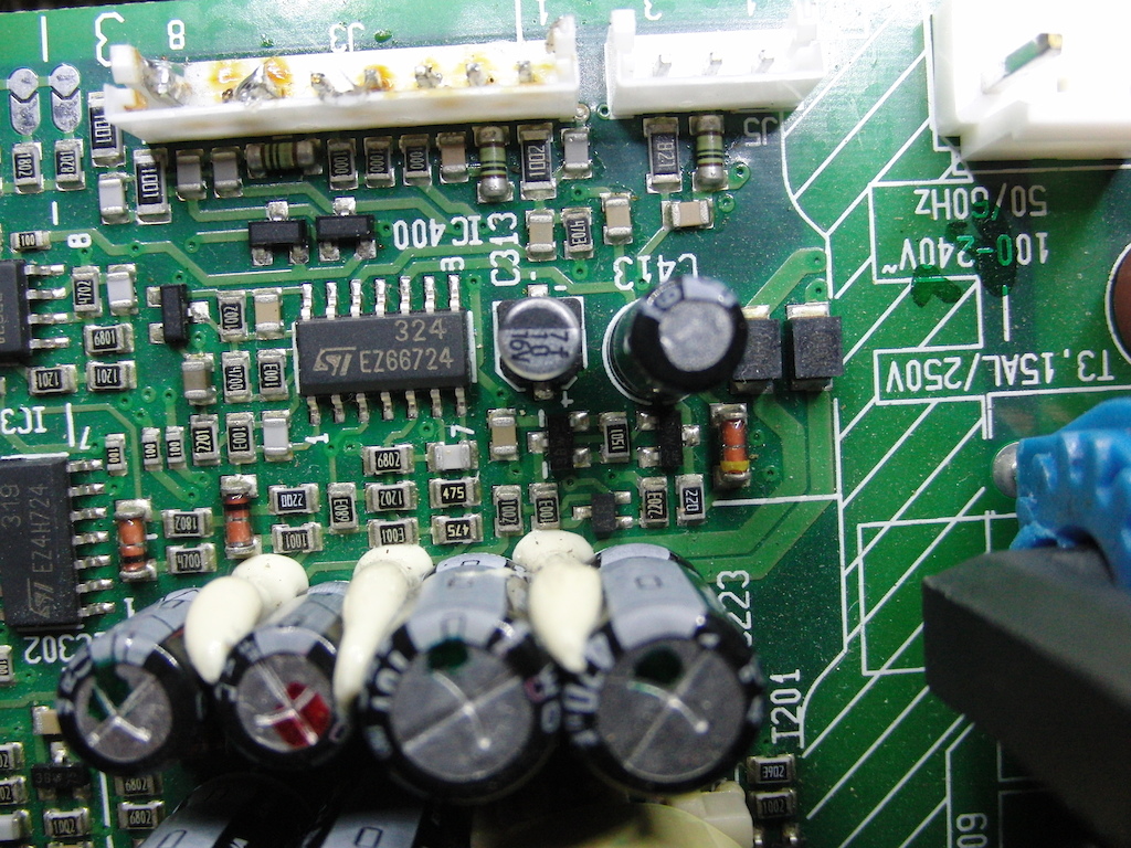
On the first image the values/writing written on top of the resistors that are pointed at.
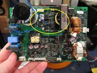
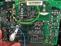
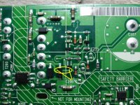
On the second image I've circled a trace, on the right hand side is the pin of a transistor and on the left hand side the trace from it terminates with a via that carries the signal to the top side of the PCB.
On my PCB this is a little different. Between the transistor and the via is a resistor, I was hoping to find out what value this was, but it looks like it's been either removed, in your version, or added, in mine. Would you be able to confirm if the transistor pin connects directly to pin 2 of the 1203D6 on the top side? It looks as if the via in your version terminates directly under the IC so I can't see where it goes from the top side image. I'm assuming it connects to pin 2 but that could be wrong.
Again many thanks!
The feedback from the optocoupler circuit is slightly simpler. As a last resort I've been thinking about remaking a small PCB just for the controller and simplifying the entire circuit surrounding it. B&Os seems unnecessarily complex compared to the application notes for the part. Whatever reason they had for adding all the extra parts it certainly didn't protect the thing from exploding.
I've taken your photos and added stuff to them to show what it is I need and a question
On the first image the values/writing written on top of the resistors that are pointed at.
On the second image I've circled a trace, on the right hand side is the pin of a transistor and on the left hand side the trace from it terminates with a via that carries the signal to the top side of the PCB.
On my PCB this is a little different. Between the transistor and the via is a resistor, I was hoping to find out what value this was, but it looks like it's been either removed, in your version, or added, in mine. Would you be able to confirm if the transistor pin connects directly to pin 2 of the 1203D6 on the top side? It looks as if the via in your version terminates directly under the IC so I can't see where it goes from the top side image. I'm assuming it connects to pin 2 but that could be wrong.
Again many thanks!
Attachments
First of all you need to determine where the problem lies with your units.
On board the PCBs are a high voltage switch mode power supply, power management for the rest of the board and then the amplifier module itself.
Any of these could be the culprit but you'd need to get your multimeter out and start testing for bad components.
The first thing to keep in mind is that there is a fuse on each board, it is the brown/red coloured short cylinder next to where the mains power enters the board. If this is dead then it has almost definitely blown due to a fault on the rest of the board. If the fuse is good then you can try measuring for some voltages.
Do always be careful as mains voltages are carried by portions of the PCB.
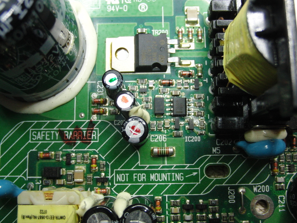
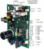
As per this picture...
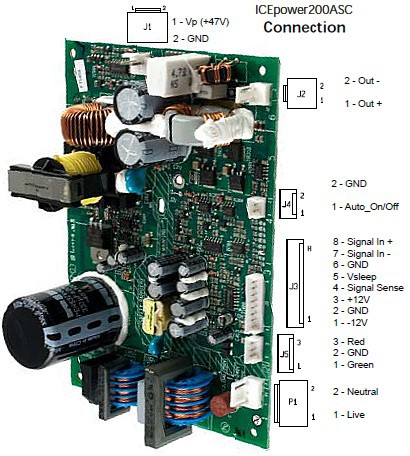
Obviously you need to power on the dead boards, but the first thing you want to do is test J1 for the presence of the main voltage rail. This is the 47V rail. Without this none of the rest of the board can function, so even when it's in standby the high voltage rail should be present.
If it is the next thing to do is test J3 for the presence of the +12 -12 and Vsleep voltages.
If those are present then the fault would be with the main amplifier.
If the J3 voltages aren't correct then either you've got a fault with the power management section or a fault in the amplifier is loading down one of the voltage rails more than they should be.
If J1 isn't present then you've more than likely got an issue with the power supply.
If the fuse is blown I'd guess that the problem would be with the power supply too. If correctly designed the PSU should limit its output current so that if the main amplifier fails and draws too much, the PSU will limit and prevent further destruction. This should prevent the fuse from blowing too, so the fuse should only blow if the PSU fails.
The first thing to test in the power supply is the main switching element, that's the big MOSFET called TR200? In the picture you posted a few posts ago.
If that's dead then the PSU is indeed dead. You'd then need to test other various components and see if they are dead or otherwise. Sometimes you need to remove a component from the circuit to be able to test it. It is also possible that there are visible signs of damage that you have not been able to spot.
On board the PCBs are a high voltage switch mode power supply, power management for the rest of the board and then the amplifier module itself.
Any of these could be the culprit but you'd need to get your multimeter out and start testing for bad components.
The first thing to keep in mind is that there is a fuse on each board, it is the brown/red coloured short cylinder next to where the mains power enters the board. If this is dead then it has almost definitely blown due to a fault on the rest of the board. If the fuse is good then you can try measuring for some voltages.
Do always be careful as mains voltages are carried by portions of the PCB.
As per this picture...
Obviously you need to power on the dead boards, but the first thing you want to do is test J1 for the presence of the main voltage rail. This is the 47V rail. Without this none of the rest of the board can function, so even when it's in standby the high voltage rail should be present.
If it is the next thing to do is test J3 for the presence of the +12 -12 and Vsleep voltages.
If those are present then the fault would be with the main amplifier.
If the J3 voltages aren't correct then either you've got a fault with the power management section or a fault in the amplifier is loading down one of the voltage rails more than they should be.
If J1 isn't present then you've more than likely got an issue with the power supply.
If the fuse is blown I'd guess that the problem would be with the power supply too. If correctly designed the PSU should limit its output current so that if the main amplifier fails and draws too much, the PSU will limit and prevent further destruction. This should prevent the fuse from blowing too, so the fuse should only blow if the PSU fails.
The first thing to test in the power supply is the main switching element, that's the big MOSFET called TR200? In the picture you posted a few posts ago.
If that's dead then the PSU is indeed dead. You'd then need to test other various components and see if they are dead or otherwise. Sometimes you need to remove a component from the circuit to be able to test it. It is also possible that there are visible signs of damage that you have not been able to spot.
Attachments

- Home
- Amplifiers
- Class D
- B&O Icepower 200ASC pictures