[h=Introduction]%1[/h]
Malefoda started the thread TDA1387 x8 DAC: let's check its design, mod it -or not-, play music -or not! - to alert everyone of the presence of a great non oversampling (NOS) DAC built around eight TDA1387 multibit DAC chips. In his blog post about the DAC, Abraxalito suggests it appears to be inspired by the Lite DAC-AH.
Overview:
[h=Availablility]%2[/h]
Note Cart100 and Taobao offer "Blue" and "Black" versions. The "Blue" version is actually a parts-only kit, while the "Black" version is completely built, ready to use out of the box. The parts-only kit version does not come with transformers, heatsinks, or a case.
Malefoda posted some links to suitable USB cards in post #11.
[h=Relevant Links]%2[/h]
[h=Modifications]%1[/h]
Roughly in order of "bang-for-buck". Easiest/most useful mods at the top. Downwards the mods increase in complexity.
[h=Op-Amp Replacement]%2[/h]
NE5534 appears to be the most common default. Swap out the NE5534s for something a bit more RF-resistant and unity gain stable.
From post #14, page 2:
So far, the AD845 (AD845JNZ) has proven to be excellent: DigiKey AD845JNZ-ND, Mouser 584-AD845JNZ.
[h=Remove 2n2 Opamp Feedback Capacitors]%2[/h]
When facing the top of the PCB, with the transformers on the right, the 2n2s are the blue film caps to the immedate left of the opamps. See post #18 on page 20 (20150211) for a picture if the description is not clear.
Quotes from Abraxalito on the 2n2 capacitors:
[h=Increase Capacitance Across TDA1387 pin7]%2[/h]
Pin7 is the tda1387 chip's reference decoupling pin. On the bottom of the board, there is a row of eight ceramic 1uF capacitors ("105"). The pole towards the transformer side of the PCB is ground, and the pole towards the I/O side of the board is pin7. See post #95 on page 10 for a picture. (Note the 100nF ("104") capacitors are for tda1387 pin5, supply voltage input.)
The ceramics should be removed, and replaced with larger electrolytics. 10v/1000uF is recommended. The electrolytic capacitors can be soldered directly to the "105" pads on the bottom of the board. But watch out for height issues! If the stock case is to be used, the electrolytic caps must be no more than 6mm in diameter, and lay perfectly flat against the PCB. Success has been reported with using two 470uF caps in parallel for this purpose. Pics of bottom-of-board pin7 electrolytic capacitor mods:
Alternatively, the electrolytic caps can be soldered on top of the board, directly to the tda1387 IC pins. The capacitor's negative pole goes to pin4 (ground), and the positive pole to pin7. Abraxalito's blog has a picture of this approach.
[h=Increase Decoupling of Analog Stage]%2[/h]
The stock DAC has two electrolytic and four film capacitors for opamp decoupling. Remove these capacitors and replace with as many 35V rated caps as you can fit. Find the lowest ESR you can get (Rubycon ZLH; Nichicon PW,HW; NCC KY, KZE). A well spec'ed recommendation: Nichicon UHW1V821MPD. Digikey 493-6928-ND, Mouser 647-UHW1V821MPD. Implementation pictures:
[h=Output Grounding Re-route]%2[/h]
The first item on Abraxalito's blog, "Re-route the output ground so the opamp filtering caps aren't subject to injected CM noise from the destination component (amp or pre)." More detail, along with an illustrative picture, on post #6 on page 1:
The pictures in post #53 on page 6 are similarly instructive.
[h=Increase TDA1387 Chip Supply Capacitance]%2[/h]
There are a couple ways to approach this (and doing both is unlikely to be a problem). The first method is analogous to the "Increase Capacitance Across TDA1387 pin7" mod above. Pin5 is the TDA1387 chip's supply voltage. You can remove the stock "104" capacitors on the back of the board and solder bigger electrolytic capacitors in their place. Post #95 on page 10 illustrates the pin5 capactors.
As of this writing, there are no pics of anyone increasing supply capacitance (pin5) on the bottom of the board. However, as with the pin7 mod, you can also solder the pin5 electrolytic caps directly to the TDA1387 IC pins on the top of the board. See post #53 on page 6 for a picture of this approach. (This picture shows added pin5 capacitance on top, directly soldered to the chip pins; and the added pin7 capacitance is on the bottom, using the "105" pads. This picture also shows added supply capacitance as described in the next paragraph.)
Another approach for adding TDA1387 IC supply capacitance is to modify the supply capacitor directly. Look again at post #53: the largest capacitor is bordred by: the heatsink to the right; the TDA1387 ICs to the top; and a big 20-pin microcontroller IC below. In this picture the cap is much larger than the stock one.
Abraxalito took this a step further, using the original capacitor's through-holes to create a "bus-bar", and hang multiple capacitors off that. From post #31 on page 4:
This can be seen in the picture on Abraxalito's blog.
[h=Opamp Constant Current Source (CCS)]%2[/h]
From post #125 on page 13:
Subsequent post #126 includes a circuit diagram plus more elaboration:
(Note the above post (#126) assumes the opamps have been removed entirely. The "four of" reference refers to one of these CCS circuits for each of the four channels (R+, L+, R-, L-) in balanced mode operation. This is an advanced modification, which will be described later in this guide.)
See post #155 on page 16 for a simplified circuit diagram of the CCS. This diagram is exactly what is needed for biasing the opamps into class-A operation; also the lines are annotated.
As for component requirements of this circuit, from post #157 on page 16:
Known working parts:
NOTE: The NOS droop fillter pictured in post #218 on page 22 is erroneous. CCS circuit attachment points to opamp pins 6 and 7 are swapped (i.e. the attachment point that should go to pin7 goes to pin6 and vice-versa).
See post #269 on page 27 for a picture of a correct CCS implementation.
[h=NOS Droop Filter]%2[/h]
Many (most? all?) NOS DACs exhibit a rolloff or "droop" at the highest frequencies, typically about -3dB at 20 kHz. Here's a discussion on Abraxalito's blog.
In post #24 on page 3, Abraxalito proposes a filter for correcting the high frequency rolloff (aka NOS droop). Further elaboration is given in post #25. Quote from those two posts:
See also post #204 on page 21 for a schematic of the NOS droop filter with annotations. Note that in that schematic, "C9999" (far right, in series with RCA connector) is the DC-blocking capacitor. The stock TDA1387 8X board already has these capacitors. They are typically square blue 2.2uF film capacitors, or in some cases axial electrolytics. If your downstream component (typically an amp) has some kind of DC-blocking mechanism (typically a series capacitor or transformer), the caps can be removed. But, if the downstream component lacks a way to block DC (e.g. a series potentiometer for volume control), the cap is needed.
As for component selection, from post #166 on page 17:
Suggested parts:
See post #218 on page 22 for pictures of a completed NOS droop filter.
See also post #219 on page 22 for pictures of another completed NOS droop filter. This is a much neater implementation, which puts the inductor on the top of the PCB, and the RC circuit on the bottom.
See also post #270 on page 27 for yet another completed NOS droop filter.
Malefoda started the thread TDA1387 x8 DAC: let's check its design, mod it -or not-, play music -or not!
- to alert everyone of the presence of a great non oversampling (NOS) DAC built around eight TDA1387 multibit DAC chips. In his blog post about the DAC, Abraxalito suggests it appears to be inspired by the Lite DAC-AH.Overview:
- DAC: Phillips TDA1387 Stereo Continuous Calibration DAC
- datasheet link 1
- datasheet link 2
- datasheet link 3 - Input voltage: 220v (Note: ebay seller "doukmall" will sell it with 110v mains if requested)
- Signal input IC: CS8416 supports TOSLINK and Coax inputs, USB support with additional daughterboard
- Output: active opamp-based I/V
[h=Availablility]%2[/h]
Note Cart100 and Taobao offer "Blue" and "Black" versions. The "Blue" version is actually a parts-only kit, while the "Black" version is completely built, ready to use out of the box. The parts-only kit version does not come with transformers, heatsinks, or a case.
- Cart100. Priced in USD, selling both "Black"/fully assembled, and "Blue"/parts-only kit.
- Taobao. Intended for domestic Chinese purchasers, but can be bought in other parts of the world through an agent.
- Ebay seller "doukmall": current link. Will supply a 110v mains version on request.
Malefoda posted some links to suitable USB cards in post #11.
[h=Relevant Links]%2[/h]
- Main DIYAudio Thread
- TDA1387 continuous calibration dac - related thread on DIYAudio
- abraxalito's blog entry on this DAC
[h=Modifications]%1[/h]
Roughly in order of "bang-for-buck". Easiest/most useful mods at the top. Downwards the mods increase in complexity.
[h=Op-Amp Replacement]%2[/h]
NE5534 appears to be the most common default. Swap out the NE5534s for something a bit more RF-resistant and unity gain stable.
From post #14, page 2:
I've buzzed out the connectivity of the opamp-DAC interface now. Its using active I/V with the opamp as a transimpedance amp. The feedback network is 620R in parallel with 2n2 and there's an output filter of 220R and 220pF. The resistors aren't the same value on mine as the silkscreen markings - my SS has 750R and 75R.
Given this new info, its clear why NE5534 is a poor choice - a transimpedance amp needs unity gain stability and 5534 doesn't have that without the Ccomp =22pF (not fitted here).
So far, the AD845 (AD845JNZ) has proven to be excellent: DigiKey AD845JNZ-ND, Mouser 584-AD845JNZ.
[h=Remove 2n2 Opamp Feedback Capacitors]%2[/h]
When facing the top of the PCB, with the transformers on the right, the 2n2s are the blue film caps to the immedate left of the opamps. See post #18 on page 20 (20150211) for a picture if the description is not clear.
Quotes from Abraxalito on the 2n2 capacitors:
abraxalito said:...Taking out the 2n2s has considerably reduced the harshness which was apparent on more complex material (orchestral strings, choral) so much that I'm not sure its still there.
...
Note that to try AD844 [opamps] you definitely need to remove the 2n2s.
...
I think the purpose of having the 2n2s across the feedback resistors is two-fold. First to limit the slewrate and secondly to provide a bit of low-pass filtering. There's a considerable downside in SQ to having them though, which isn't expected under the normal ways of understanding opamp behaviour. I suspect it has something to do with putting glitches on the supply rails when they're present.
...
If you were only to do one mod, the most significant one I'd say for listening pleasure is deleting those feedback caps (2n2s) around the opamps. That kills a lot of the harshness and improves the depth.
[h=Increase Capacitance Across TDA1387 pin7]%2[/h]
Pin7 is the tda1387 chip's reference decoupling pin. On the bottom of the board, there is a row of eight ceramic 1uF capacitors ("105"). The pole towards the transformer side of the PCB is ground, and the pole towards the I/O side of the board is pin7. See post #95 on page 10 for a picture. (Note the 100nF ("104") capacitors are for tda1387 pin5, supply voltage input.)
The ceramics should be removed, and replaced with larger electrolytics. 10v/1000uF is recommended. The electrolytic capacitors can be soldered directly to the "105" pads on the bottom of the board. But watch out for height issues! If the stock case is to be used, the electrolytic caps must be no more than 6mm in diameter, and lay perfectly flat against the PCB. Success has been reported with using two 470uF caps in parallel for this purpose. Pics of bottom-of-board pin7 electrolytic capacitor mods:
- post #53 on page 6 (only one set of 470uF caps)
- post #120 on page 12
- post #121 on page 13
Alternatively, the electrolytic caps can be soldered on top of the board, directly to the tda1387 IC pins. The capacitor's negative pole goes to pin4 (ground), and the positive pole to pin7. Abraxalito's blog has a picture of this approach.
[h=Increase Decoupling of Analog Stage]%2[/h]
The stock DAC has two electrolytic and four film capacitors for opamp decoupling. Remove these capacitors and replace with as many 35V rated caps as you can fit. Find the lowest ESR you can get (Rubycon ZLH; Nichicon PW,HW; NCC KY, KZE). A well spec'ed recommendation: Nichicon UHW1V821MPD. Digikey 493-6928-ND, Mouser 647-UHW1V821MPD. Implementation pictures:
- post #186 on page 19 - second picture shows a stock board on the left, and a modified board on the right.
- post #194 on page 20
- post #53 on page 6
[h=Output Grounding Re-route]%2[/h]
The first item on Abraxalito's blog, "Re-route the output ground so the opamp filtering caps aren't subject to injected CM noise from the destination component (amp or pre)." More detail, along with an illustrative picture, on post #6 on page 1:
Taking a look at the layout there could be a common-mode noise problem in that there are a couple of 220pF caps feeding directly into the opamps' +ve inputs from a dirty ground (the output ground). So first things first, I shall cut the thick track along the red line and route the output ground back to the trafo (indicated by the green arrow).
The pictures in post #53 on page 6 are similarly instructive.
[h=Increase TDA1387 Chip Supply Capacitance]%2[/h]
There are a couple ways to approach this (and doing both is unlikely to be a problem). The first method is analogous to the "Increase Capacitance Across TDA1387 pin7" mod above. Pin5 is the TDA1387 chip's supply voltage. You can remove the stock "104" capacitors on the back of the board and solder bigger electrolytic capacitors in their place. Post #95 on page 10 illustrates the pin5 capactors.
As of this writing, there are no pics of anyone increasing supply capacitance (pin5) on the bottom of the board. However, as with the pin7 mod, you can also solder the pin5 electrolytic caps directly to the TDA1387 IC pins on the top of the board. See post #53 on page 6 for a picture of this approach. (This picture shows added pin5 capacitance on top, directly soldered to the chip pins; and the added pin7 capacitance is on the bottom, using the "105" pads. This picture also shows added supply capacitance as described in the next paragraph.)
Another approach for adding TDA1387 IC supply capacitance is to modify the supply capacitor directly. Look again at post #53: the largest capacitor is bordred by: the heatsink to the right; the TDA1387 ICs to the top; and a big 20-pin microcontroller IC below. In this picture the cap is much larger than the stock one.
Abraxalito took this a step further, using the original capacitor's through-holes to create a "bus-bar", and hang multiple capacitors off that. From post #31 on page 4:
I've just put a dent in one remaining weakness of this DAC - the bass. Its a very simple mod to add capacitance to the TDA1387's supply. I soldered some 1.5mm copper wire to the two pads for the lytic (just beneath the chips in Matthieu's pic) and used that wire as 'bus-bar' to solder across 4 * 15,000uF 6.3V Panasonic NHG caps in a horizontal position. This tightens up the bass nicely.
This can be seen in the picture on Abraxalito's blog.
[h=Opamp Constant Current Source (CCS)]%2[/h]
From post #125 on page 13:
I'd suggest current sources on the opamp outputs as with an array of 8 DACs the opamps have to source or sink up to 8mA, well beyond classA operation of the output stage. I use the traditional two transistor current source and it goes between the opamp output pin (pin6) and the -ve supply rail.
Subsequent post #126 includes a circuit diagram plus more elaboration:
Here's the schematic for the classA buffer I'm using (four of) in the latest DAC mods. The two transistors at the bottom form a constant current source - its this CCS which can also be used to bias an opamp into classA. The bias current is set here by the 82R resistor for about 8mA. The transistors are literally 'two a penny' types in SOT23.
(Note the above post (#126) assumes the opamps have been removed entirely. The "four of" reference refers to one of these CCS circuits for each of the four channels (R+, L+, R-, L-) in balanced mode operation. This is an advanced modification, which will be described later in this guide.)
See post #155 on page 16 for a simplified circuit diagram of the CCS. This diagram is exactly what is needed for biasing the opamps into class-A operation; also the lines are annotated.
As for component requirements of this circuit, from post #157 on page 16:
Not all transistors will perform as well here - I look for a couple of parameters. First is 'hoe' the output impedance, indicated in Spice models by the parameter 'VAF' - we want a high number as ideally a CS has infinite output impedance. Second we don't want the transistor to have a much lower 'hoe' close to its saturation region - this can be seen on the traditional transistor curve tracer plots. I'll post up some pics later to demonstrate what's important. I don't know about Digikey's pricing but the BC817 (its a SOT23, there are leaded equivalents) is one of the cheapest going - I got a reel of them (3k) and the price was under $30 so less than a cent each.
As for resistors - almost anything will do, I'm using 0805 thick film without noticeable problems. I wouldn't advise 0603 as they do get rather noisy at higher values (like 33k). Leaded metal film will likely have better performance but as for whether you'd notice it, I can't say.
Known working parts:
- Transistor: Fairchild Semiconductor BC33740TA DigiKey BC33740TACT-ND, Mouser 512-BC33740TA
- 33kohm Resistor: TE Connectivity / Neohm LR1F33K Mouser 279-LR1F33K
- 82ohm Resistor: Yageo MFR50SFTE52-82R Mouser 603-MFR50SFTE52-82R
NOTE: The NOS droop fillter pictured in post #218 on page 22 is erroneous. CCS circuit attachment points to opamp pins 6 and 7 are swapped (i.e. the attachment point that should go to pin7 goes to pin6 and vice-versa).
See post #269 on page 27 for a picture of a correct CCS implementation.
[h=NOS Droop Filter]%2[/h]
Many (most? all?) NOS DACs exhibit a rolloff or "droop" at the highest frequencies, typically about -3dB at 20 kHz. Here's a discussion on Abraxalito's blog.
In post #24 on page 3, Abraxalito proposes a filter for correcting the high frequency rolloff (aka NOS droop). Further elaboration is given in post #25. Quote from those two posts:
Here's a filter I'm going to try after the opamp - its designed to do two things. First correct for the NOS droop and second attenuate OOB images produced by the DAC. The filter that's currently on the opamp output (220R, 220pF) has a -3dB over 3MHz so isn't doing much (if anything at all) to tame the DAC's images. My filter's 2 pole and it provides 24dB attenuation at 100kHz. The inductor's a Coilcraft MSS1210. The 50k resistor isn't part of the filter itself, its my volume pot
...
I've been listening now for an hour or so and this filter's definitely for keeps. The rise in HF response makes it sound just a tad more transparent and I'm getting more of an 'in focus' sound, closer to my reference DAC.
See also post #204 on page 21 for a schematic of the NOS droop filter with annotations. Note that in that schematic, "C9999" (far right, in series with RCA connector) is the DC-blocking capacitor. The stock TDA1387 8X board already has these capacitors. They are typically square blue 2.2uF film capacitors, or in some cases axial electrolytics. If your downstream component (typically an amp) has some kind of DC-blocking mechanism (typically a series capacitor or transformer), the caps can be removed. But, if the downstream component lacks a way to block DC (e.g. a series potentiometer for volume control), the cap is needed.
As for component selection, from post #166 on page 17:
For the caps, I've used NP0 ceramics but they're SMT, you could use pretty much any film caps (steer away from mylar though) [if you] want leaded... Resistors - standard metal film leaded will be superior to the thick film that I've used.
Suggested parts:
- L30 10mH Inductor: Coilcraft MSS1210-106KEB, Mouser 994-MSS1210-106KEB (seem to be only available direct from Coilcraft, at least in the USA)
- C43 220nF Capacitor: WIMA MKS2C032201B00KSSD, Mouser 505-MKS2C032201B00KS
Alternate: WIMA MKP10-.22/250/5P15, Mouser 505-MKP10-.222505P15 - C42 4nF Capacitor: Kemet PHE426DJ4390JR05, Mouser 80-PHE426DJ4390JR05
Alternate: Panasonic ECW-HA3C392H4, Mouser 667-ECW-HA3C392H4, DigiKey ECW-HA3C392H4-ND - R55 33 ohm Resistor: Yageo MFR50SFTE52-33R, Mouser 603-MFR50SFTE52-33R
- R54 2.2 kohm Resitor: KOA Speer MFS1/2DCT52R2201F, Mouser 660-MFS1/2DCT52R2201
See post #218 on page 22 for pictures of a completed NOS droop filter.
See also post #219 on page 22 for pictures of another completed NOS droop filter. This is a much neater implementation, which puts the inductor on the top of the PCB, and the RC circuit on the bottom.
See also post #270 on page 27 for yet another completed NOS droop filter.
Dear abraxalito,
Thank you for your guidance and research !
Have ordered a TDA1387 L1387DAC 8X Dac through Taobao using an agent. Purchased with the CM6631 24bit 192k USB asynchronous daughter card. Will tell you when received and I will order the AD845 Op-Amps.
All the best
Thank you for your guidance and research !
Have ordered a TDA1387 L1387DAC 8X Dac through Taobao using an agent. Purchased with the CM6631 24bit 192k USB asynchronous daughter card. Will tell you when received and I will order the AD845 Op-Amps.
All the best
Last edited:
Ha, great to hear this DAC is still available and getting interest. Do let us know about how it sounds and any mods you do
Thank you abraxalito !
Pairing the TDA1387 L1387DAC 8X Dac with a JLH Headphone Amp from Ebay
Is it possible to use USB to I2S with the TDA1387 8X Dac ? Looking at buying the DIYINHK USB to I2S.
Thank you !
Thank you !
The DAC already has a header for fitting a USB interface, if you contact the vendor maybe he can supply you with the necessary board to plug in.
https://item.taobao.com/item.htm?sp...877&pvid=69bceeda-95e2-47ba-9f2b-72fd6b377375
He gives the links to the interface boards on that page but they're not allowed to be URLs by Taobao's rules so you have to cut and paste them into your browser. Here's the first one - https://item.taobao.com/item.htm?spm=686.1000925.1000774.115.vvnzQ0&id=35523381322
Last edited:
1. If you want to upgrade the opamps you'll need 2 * AD845.
2. I have several DAC AH and one of the first mods I do is snipping out all the 1543s. I've replaced them with TDA1545A (in DIL8) in some but that chip doesn't sound as good as TDA1387. In stock form the DAC AH is less fatiguing but even just snipping out the 2n2 feedback caps and swapping the opamps gives the TDA1387 DAC the edge. The DAC AH has a nicer and more robust PCB.
2. I have several DAC AH and one of the first mods I do is snipping out all the 1543s. I've replaced them with TDA1545A (in DIL8) in some but that chip doesn't sound as good as TDA1387. In stock form the DAC AH is less fatiguing but even just snipping out the 2n2 feedback caps and swapping the opamps gives the TDA1387 DAC the edge. The DAC AH has a nicer and more robust PCB.
I see that Audiophonics is selling a 8x TDA1387 DAC for the RPi. Has anyone tried it or got more information about it than exists on the web page? AUDIOPHONICS I-TDA1387 TCXO DAC Raspberry Pi 3 / A+ B+ / Pi 2 / I2S - Audiophonics
It looks quite similar to this Chinese designed one - perhaps its a near-clone : https://item.taobao.com/item.htm?spm=a230r.1.14.60.UTuJh4&id=538116703620&ns=1&abbucket=18#detail
It looks quite similar to this Chinese designed one - perhaps its a near-clone : https://item.taobao.com/item.htm?spm=a230r.1.14.60.UTuJh4&id=538116703620&ns=1&abbucket=18#detail
Thanks, I hadn't seen that one. I don't see any opamps in there. Are there any recommendations for mods to this version anywhere?
Just today received the Audiophonics TDA1387 x8 dac for the pi. Listening to it for only an hour, first impressions, it's smooth. A bit more transparency would be welcome, maybe that will be the case with a few more days running. Or just let it warm up! Call me impressed for a 1990's dac chip... It's "listening" good so far
I've had one here since early this year, but haven't tried it yet. I'd REALLY like to understand why they included a 50Mhz clock on the board and what they use it for. I've asked and gotten 2 nonsense useless answers. I asked:
"I do not understand how you use the 50Mhz TCXO. When I read the datasheet the TDA1387 only needs the I2S Data, LRCK, and BCK to work. What does the 50Mhz clock do?"
And got back:
"It's right.
Normaly in the TDA1541 we have the SCK input in pin 4.
On the TDA1387 the TCXO input in the logical door to distribute to the 8X TDA 1387. We think the signal is matrix in the BCK / SLK and DATA like an spdif..
We asked to the designer for a more accurate answer. When we have the better answer. I wil send to you an email."
and when I asked again
"Did you ever get additional information on the purpose of the 50mHz clock on your TDA1387 DAC?"
I got:
"This DAC is a slave and need a clock to work correctly (50mhz clock are common for 192khz decoding)."
Both are nonsense answers AFAIK. Anyone know why and how?
Greg in Mississippi
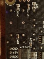
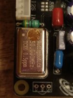
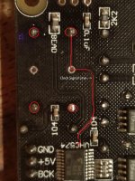
Nope, right on the board and it looks like the clock signal is input to the VHC574 that I suspect is used for distributing the I2S signals to the DAC chips. I'll have to download the VHC574 datasheet and trace things a bit, I guess.
Since this chip doesn't have ASRC like the ESS ones, a single clock frequency doesn't make sense, especially when it is not integer-related to any of the sampling frequencies.
If it is used to reclock the distribution of the I2S signals, I'd be tempted to un-power the clock and route the clock signal from an Allo.com Kali to the VCH574 to accomplish the same, but at least using a sampling-frequency-related clock.
I've posted closeup pix of the clock and the board under the clock showing the output trace going to the VHC574.
Greg in Mississippi
P.S. Did crude MS Paint markup to show clock pins and clock output signal line.
P.P.S. And you are right, passive I/V with bipolar Nichicon Muse ES caps for coupling caps. There's room for improvement.
Attachments
Last edited:
- Status
- This old topic is closed. If you want to reopen this topic, contact a moderator using the "Report Post" button.
- Home
- diyaudio.com Wiki
- TDA1387 X8 NOS DAC