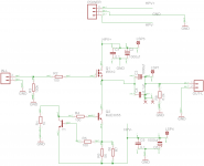
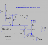
I have attached the schematic and board layout for the buffer. I plan to copy and make 2 channels on the same pcb and use a single heatsink (along the length of the pcb) for all the 4 transistors. Any issues with this.
Do I need both R4 and R5 for ring of two ccs stability.
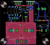
How does the layout look.
Do I need both R4 and R5 for ring of two ccs stability.
How does the layout look.
Attachments
Hi,
You may omit with R4. R5 has negligible impact and may be raised to 1k.
C3 should be a bipolar cap.
optional:
- You may split R1 in two resistors with increased value (5K-10k) and add a cap of a few µF from the resistor mid-joint to the negative supply.
- You can omit with the output coupling caps using a active DC-servo that controls the idle current of the ccs, and a bias voltage and a source resistor for the MOSFET.
For an example of the servo circuit see my website calvins-audio-page.jimdo.com/ideas-and-circuits/buffers/hybrid-buffer-en/.
Scroll down to "Calvin-Buffer plus dc-servo".
jauu
Calvin
I have seen this suggestion somewhere else also, but I also see plenty of people using polarized caps at the output. I can see why it should be bipolar, as even with 4v dc, if I use 600 ohms headphones, output could go upto say 8v, then the cap will have reverse voltage on it. But then how come people use polarized caps at headphone amp output. Will a polarized cap be damaged at the output.Hi,
You may omit with R4. R5 has negligible impact and may be raised to 1k.
C3 should be a bipolar cap.
In sims, didnt show any advantage, but then i am not simulating ripple etc. is it to improve the psrr.optional:
- You may split R1 in two resistors with increased value (5K-10k) and add a cap of a few µF from the resistor mid-joint to the negative supply.
- You can omit with the output coupling caps using a active DC-servo that controls the idle current of the ccs, and a bias voltage and a source resistor for the MOSFET.
For an example of the servo circuit see my website calvins-audio-page.jimdo.com/ideas-and-circuits/buffers/hybrid-buffer-en/.
Scroll down to "Calvin-Buffer plus dc-servo".
jauu
Calvin
from what I read about the dc servo examples so far, it doesnt seem to work so well in controlling large offsets in a small time frames. I need that as the output will have some 3.5-4v of dc, enough to damage the headphones very fast. Any solutions for this? BTW, how long can 32 ohm headphones handle 4v dc, which is about twice the power that they can handle.
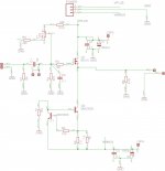
I tried the other approach of using a pot to bias the gate to remove the dc. I have attached the schematic for that (r9 and r10 are for setting input impedance to about 47k, i might have to tweak the values a bit). Wont this approach degrade the psrr of the system. If I am injecting 3.5v from a 15v supply into the gate of a unity gain mosfet, thats just 6db below what the power supply will give. is it really worth it to get rid of the output cap at that cost.
Attachments
Last edited:
The schematic in post 6 will have 20-30% of the positive rail noise at the input of the mosfet. It comes down to the voltage division of the values chosen. As is there would be ~55% of the noise appearing across P1. So if you have say 100mV of noise on the B+, P1 would have ~55mV appear across pins 1 and 3. If the pin 2 wiper happened to bias up correctly at 50%, then 27mV of the noise would appear at pin 2 which is also the gate of the mosfet.
Using a low impedance voltage reference like the one attached can reduce that 27mV down to around 50uV. It would also give a reliable bias voltage even if the rail voltage fluctuates.
Using a low impedance voltage reference like the one attached can reduce that 27mV down to around 50uV. It would also give a reliable bias voltage even if the rail voltage fluctuates.
Attachments
Last edited:
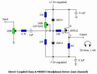
He's copying the direct-coupled version of the Szekeres circuit. Headwize is down at the moment, so I'll attach the circuit.
It was never intended to be a low noise anything, just quick'n'dirty. Most people will use regulated supplies however, so sufficient improvement can be obtained by simply adding a large cap from the pot wiper to ground and a large resistor between the pot wiper and the R3-R4 node. R3 and C2 can be removed.
It was never intended to be a low noise anything, just quick'n'dirty. Most people will use regulated supplies however, so sufficient improvement can be obtained by simply adding a large cap from the pot wiper to ground and a large resistor between the pot wiper and the R3-R4 node. R3 and C2 can be removed.
Attachments
Last edited:
I imagine its hard for you all to imagine how much I hate this circuit.
No disrespect to Greg Szekeres. He knew what he was doing ... indeed that's the problem: he took the circuit exactly as far as it could/should go, not a hair further. Any further mucking around with it just ends up in frustration ... the basic circuit element just isn't good enough to make improvements worthwhile.
First, the PSRR, distortion, heck just about any metric you care to name - is just natively sucky. Second, trying to drive a MOSFET from a volume control is just a dumb idea. Third, the power conversion efficiency is so low its borderline criminal. If was was going to generate so much heat to drive headphones with high distortion I'd at least have the courtesy to use a vacuum tube so as to have some sort of excuse when the IPCC came calling.
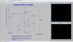
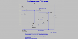
Anyhow, I felt compelled to give it (yet another) go round, since its been some years since my last attempt. I'd go with a CSS, as the OP had. I'd tidy up the bias network however, and reduce the input coupling cap (might as well, it makes the nice ones more affordable). Playing with the LTSpice sim, however, confirmed that as "high performance audio" its basically a lost cause.
For all that it sounds perfectly fine though. Well, a bit muddy, but many people won't mind that.
note: replace Q1 Q2 with something like BD135 which can take the power dissipation.
No disrespect to Greg Szekeres. He knew what he was doing ... indeed that's the problem: he took the circuit exactly as far as it could/should go, not a hair further. Any further mucking around with it just ends up in frustration ... the basic circuit element just isn't good enough to make improvements worthwhile.
First, the PSRR, distortion, heck just about any metric you care to name - is just natively sucky. Second, trying to drive a MOSFET from a volume control is just a dumb idea. Third, the power conversion efficiency is so low its borderline criminal. If was was going to generate so much heat to drive headphones with high distortion I'd at least have the courtesy to use a vacuum tube so as to have some sort of excuse when the IPCC came calling.
Anyhow, I felt compelled to give it (yet another) go round, since its been some years since my last attempt. I'd go with a CSS, as the OP had. I'd tidy up the bias network however, and reduce the input coupling cap (might as well, it makes the nice ones more affordable). Playing with the LTSpice sim, however, confirmed that as "high performance audio" its basically a lost cause.
For all that it sounds perfectly fine though. Well, a bit muddy, but many people won't mind that.
note: replace Q1 Q2 with something like BD135 which can take the power dissipation.
Attachments
Last edited:
The distortion and frequency response is pretty much what you would expect, my gripe would again be the bias network. Noise aside, only the top 20% of the pot's range is usable, which may be "ok" with a 10 turn. A more stable bias generator/offset compensation would be preferred if using dc coupling with headphones.
Not sure why do you have such problems with class A amp. All followers work like this. But for headphone it is still not much heat. I managed to get thd to around 0,02%. But on paper all schematics work like a charm.
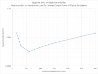
0.02% isn't very informative without quoting the power output and impedance range of the load.
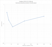
For a reasonable 10 mW into 16-300 ohms, I'd have to spec my version at 0.4%. Best case is 0.07% for 60 ohms. I challenge you to do substantially better without burning more than 2 W per channel. As jerluwoo says, its what you expect for this circuit topology. That's my problem with it: it just isn't very good to start with. (The bias network of the OP only degrades it further.)
(I've included the same data for a push-pull class A design (Sapphire 3.0f3) running at less than half the bias current for educational purposes only.)
Attachments
Last edited:
Member
Joined 2009
Paid Member
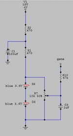
I changed the bias network to use led as reference. Is 1uf good for C2, I get a lot more stable voltage at the pot viper with a larger cap, say 100uf. Is the bias network ground supposed to connect to input signal ground on the pcb, not sure if its such a good idea to use that ground for the LED current (which is currently set to about 10ma).
I also reduced the supply voltage from 15v to 12v to reduce power dissipation in the transistors. The Iq is about 230ma. the transistors are dissipating about 2.5w each. bc550c is running at 50ma and about 75mw.
I get about 0.155% distortion while giving about 2.63v into 32 ohms.
I also reduced the supply voltage from 15v to 12v to reduce power dissipation in the transistors. The Iq is about 230ma. the transistors are dissipating about 2.5w each. bc550c is running at 50ma and about 75mw.
I get about 0.155% distortion while giving about 2.63v into 32 ohms.
Attachments
Is the bias network ground supposed to connect to input signal ground on the pcb, not sure if its such a good idea to use that ground for the LED current (which is currently set to about 10ma).
You could try that, but the filtered voltage across C2 and R6 is an input signal,
so C2 and R6 should be grounded with the input on the pcb.
Post17:
C3 goes to V-, not to audio ground.
R11 & 12 look quite low. You don't need 10 to 12mA for a mosFET bias circuit.
The Blue LEDs would be better replaced with 4, or 5, Red LEDs. 1mA to 2mA would be enough for the Red LEDs allowing 1k, or more, to be used.
C5/R8 roll off the bass a bit high.
R8 could be increased to around 100k to 220k
Q2 can be set to somewhere between 2mA and 10mA. 50mA is too high.
You might need a base stopper or two to stabilise the 2q CCS
I wonder if you have your Audio grounding mixed up with your Power grounding.
You are using the same symbol for all !
Absolute max output will be around 7Vac to 8Vac with +-12Vdc supplies.
Consider around -12dB (1/4) as the normal maximum audio signal.
I'd suggest that for this single ended source follower you look at maximum audio signals of <=1.9Vac, or increase you supplies back to +-15Vac to allow 2.2Vac from a CDP to be passed with acceptable distortion.
Last edited:
But if you do need >10 mA (current gain on ye olde '3055 isn't so fantabulous, ), use a medium-power transistor, BC337 or whatnot.Q2 can be set to somewhere between 2mA and 10mA. 50mA is too high.
He was clearly asking about grounding in that very same post, wasn't he? You can always insert some R and L and define additional ground nodes.I wonder if you have your Audio grounding mixed up with your Power grounding.
You are using the same symbol for all !
I don't think that factor-of-4 rule of thumb really applies to CCS-loaded followers. With the CCS the main source of voltage depence has been just about eliminated, and distortion into higher-impedance loads is much improved. These things hence tend to be limited by current rather than voltage swing. The only voltage effects remaining would be capacitance nonlinearity and Early effect.Absolute max output will be around 7Vac to 8Vac with +-12Vdc supplies.
Consider around -12dB (1/4) as the normal maximum audio signal.
I'd suggest that for this single ended source follower you look at maximum audio signals of <=1.9Vac, or increase you supplies back to +-15Vac to allow 2.2Vac from a CDP to be passed with acceptable distortion.
Besides, 2 Vrms tends to be enough to blow your ears off with many headphones anyway, and I'd much rather see a need for a volume control somewhere.
I'm not sure whether output DC offset stability will suffice in this circuit, and would not be surprised to see warmup drift well in the 10s of mV, maybe even more. This sort of buffer normally tends to be used either with a capacitor-coupled output or within a feedback loop, where a bit of drift is not critical at all. RJM addressed this problem in his improved Szekeres by using a third MOSFET for an active ground channel, all 3 being hand-matched for Vgs drop. It's not like I'd be that fond of the idea though, output impedance of the ground channel buffer sims at >2 ohms at 75 mA with IRF510 (though only half that for a '530) and would add to ground return impedance. I would advise to keep the latter below 1/30 of load impedance, ideally 1/100. Like RocketScientist/NwAvGuy wrote, real ground beats virtual ground.
- Home
- Amplifiers
- Headphone Systems
- class A Buffer