Just an idea that popped up during some browsing through all the class A threads, showing BIG amplifiers and BIG heatsinks to get SOME power for your speakers.
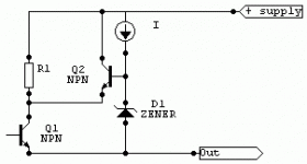
It is about a push-pull output stage using emitter followers, where only the top half of the output circuit is shown, using an NPN transistor. The other half can be a PNP mirror of this.
What if we keep the output transistor (Q1) in class A at high current but limit the voltage across the transistor? This keeps the dissipation limited, so less transistors needed in parallel and a smaller heatsink. But of course we want reasonable voltage swing and thus need a power supply with a less limited voltage. If we now insert a power resistor (R1) in between the collector of the output transistor and the supply line, this resistor can dissipate most of the power that would otherwise be dissipated in the output transistor. Because a resistor is allowed to be much hotter than a transistor, in this way more power can be dissipated in a smaller volume. Do not mount the resistor on the same heatsink as the transistor, though.
But as soon as the base of Q1 goes up and Q1 needs to deliver current to the load, Vce of Q1 may become too small and Q1 would saturate. Here Q2 comes into action. It is a kind of cascode for Q1 and is driven from the output via D1. Current beyond the bias current of Q1 will be delivered via Q2. Probably even part of the bias current of Q1 is already delivered by Q2 and part by R1. Q2 keeps Vce1 at a voltage of Vz-Vbe2. Current source I keeps the zener diode biased and supplies the base current for Q2.
I have not started making calculations (nor simulations) for this setup to determine where the optimum is. I think we should strive for a situation where most of the dissipation is in R1 and some in Q1 and Q2 for most of the time, normally when signal levels are low.
This circuit may also improve linearity of the class A amp because Vce1 is kept fairly constant for all signal levels.
This circuit may also be interesting for class AB amplifiers hat drive capacitive loads. For capacitive loads the output current is already large for small output voltages, making the dissipation in Q1 large (large Vce, large Ic). Insertion of R1 will then lower Vc1. For class AB amplifiers Ic1-bias will be low, so the voltage across R1 will be low with no signal. In order not to reverse bias Q2 it will be required to insert a diode in the base of Q2, otherwise emitter-base zenering will occur.
I don't know if this circuit is new. I did a quick search, but could not find the right keywords for a usefully limited answer. I just post it on the forum to see what happens.
Steven
It is about a push-pull output stage using emitter followers, where only the top half of the output circuit is shown, using an NPN transistor. The other half can be a PNP mirror of this.
What if we keep the output transistor (Q1) in class A at high current but limit the voltage across the transistor? This keeps the dissipation limited, so less transistors needed in parallel and a smaller heatsink. But of course we want reasonable voltage swing and thus need a power supply with a less limited voltage. If we now insert a power resistor (R1) in between the collector of the output transistor and the supply line, this resistor can dissipate most of the power that would otherwise be dissipated in the output transistor. Because a resistor is allowed to be much hotter
than a transistor, in this way more power can be dissipated in a smaller volume. Do not mount the resistor on the same heatsink as the transistor, though. But as soon as the base of Q1 goes up and Q1 needs to deliver current to the load, Vce of Q1 may become too small and Q1 would saturate. Here Q2 comes into action. It is a kind of cascode for Q1 and is driven from the output via D1. Current beyond the bias current of Q1 will be delivered via Q2. Probably even part of the bias current of Q1 is already delivered by Q2 and part by R1. Q2 keeps Vce1 at a voltage of Vz-Vbe2. Current source I keeps the zener diode biased and supplies the base current for Q2.
I have not started making calculations (nor simulations) for this setup to determine where the optimum is. I think we should strive for a situation where most of the dissipation is in R1 and some in Q1 and Q2 for most of the time, normally when signal levels are low.
This circuit may also improve linearity of the class A amp because Vce1 is kept fairly constant for all signal levels.
This circuit may also be interesting for class AB amplifiers hat drive capacitive loads. For capacitive loads the output current is already large for small output voltages, making the dissipation in Q1 large (large Vce, large Ic). Insertion of R1 will then lower Vc1. For class AB amplifiers Ic1-bias will be low, so the voltage across R1 will be low with no signal. In order not to reverse bias Q2 it will be required to insert a diode in the base of Q2, otherwise emitter-base zenering will occur.
I don't know if this circuit is new. I did a quick search, but could not find the right keywords for a usefully limited answer. I just post it on the forum to see what happens.
Steven
Attachments
johnferrier said:Bob Carver patented the idea of using three different +/- supply rails and switches in only the amount of voltage needed.
I know, that is 3-stage class G. But then you get voltage jumps on the collector of Q1, which show up as a kind of crossover distortion at the output for each transistion to another power rail. With 3 positive and 3 negative supply rails you get 5 transitions that may generate crossover distortion. The purpose of class G is to make the amplifier more efficient. My circuit is not more efficient but only moves part of the heat to a resistor that is more capable of dissipating than a transistor. Also the circuit does not have any transition 'areas' that could introduce distortion.
john curl said:Has been tried before, maybe patented by Nelson Pass.
Any references, you know of?
Steven
Steven said:Also the circuit does not have any transition 'areas' that could introduce distortion.
Steven
would you get any distortion as Q2 starts to kick in?
U.S. Patent #5,343,166, which can be viewed by doing a patent number search at www.uspto.gov.Steven said:Any references, you know of?
Steven said:Just an idea that popped up during some browsing through all the class A threads, showing BIG amplifiers and BIG heatsinks to get SOME power for your speakers.
It is about a push-pull output stage using emitter followers, where only the top half of the output circuit is shown, using an NPN transistor. The other half can be a PNP mirror of this.
What if we keep the output transistor (Q1) in class A at high current but limit the voltage across the transistor? This keeps the dissipation limited, so less transistors needed in parallel and a smaller heatsink. But of course we want reasonable voltage swing and thus need a power supply with a less limited voltage. If we now insert a power resistor (R1) in between the collector of the output transistor and the supply line, this resistor can dissipate most of the power that would otherwise be dissipated in the output transistor. Because a resistor is allowed to be much hotter
But as soon as the base of Q1 goes up and Q1 needs to deliver current to the load, Vce of Q1 may become too small and Q1 would saturate. Here Q2 comes into action. It is a kind of cascode for Q1 and is driven from the output via D1. Current beyond the bias current of Q1 will be delivered via Q2. Probably even part of the bias current of Q1 is already delivered by Q2 and part by R1. Q2 keeps Vce1 at a voltage of Vz-Vbe2. Current source I keeps the zener diode biased and supplies the base current for Q2.
I have not started making calculations (nor simulations) for this setup to determine where the optimum is. I think we should strive for a situation where most of the dissipation is in R1 and some in Q1 and Q2 for most of the time, normally when signal levels are low.
This circuit may also improve linearity of the class A amp because Vce1 is kept fairly constant for all signal levels.
This circuit may also be interesting for class AB amplifiers hat drive capacitive loads. For capacitive loads the output current is already large for small output voltages, making the dissipation in Q1 large (large Vce, large Ic). Insertion of R1 will then lower Vc1. For class AB amplifiers Ic1-bias will be low, so the voltage across R1 will be low with no signal. In order not to reverse bias Q2 it will be required to insert a diode in the base of Q2, otherwise emitter-base zenering will occur.
I don't know if this circuit is new. I did a quick search, but could not find the right keywords for a usefully limited answer. I just post it on the forum to see what happens.
Steven
Steven,
I have done a design like that for Audio Amateur in the 80's, but without the resistor. The main advantage of my design was that the output transistors could be selected for linearity and high bandwidth, while the "regulator' transistor can be selected for robustness and high power dissipation. The result is that the supply for the output transistors shows signal-related ripple, but that can be taken care of by having a good PSRR in the main amp channel. Worked quite well.
Jan Didden
Re: Re: Spreading the heat in class A
No need to kick in for Q2. It can be conducting all the time (in class A). Both R1 and Q2 take care of the current through Q1.
I found this patent too this morning (in Europe), but had no time to answer. Still thanks.
This patent describes something else, although on first sight it has some similarities. Patent #5,343,166 from Nelson Pass describes a floating current source powered from an additional (low voltage, high current) power supply that sources a current through Q1 in order to keep Q1 in class A and to minimize the current through Q2 because that would cause a lot of dissipation in Q2 which runs on a higher voltage. Purpose of this circuit is then to get a higher efficiency. Q1 and Q2 are not mentioned in the patent, but are the equivalents in my diagram. Numbering in the patent is completely different. The patent does not use resistors, as in my circuit R1. The only reference to a resistor in this sense is in column 3 at the bottom: "Alternatively, the high source impedance of the current source could be provided by a resistor." But what is meant in the patent is that you can have a floating power supply with a series resistor to increase the impedance across Q1. The impedance should be high because the voltage across Q1 is fixed by Q2 and the zenerdidode, and these two should not interfere.
As already said, the purpose of my circuit is not to get a higher efficiency but only to move part of the dissipation to a resistor. I do not use an additional floating power supply.
This is more in line with the original patent of Nelson Pass 4,107,619 that uses a cascode on the output transistors to keep the Vce of each output transistor nearly constant. There is no resistor R1 that takes over part of the dissipation. The advantage of improved linearity is still part of my circuit, since I use the cascode too.
Steven
millwood said:would you get any distortion as Q2 starts to kick in?
No need to kick in for Q2. It can be conducting all the time (in class A). Both R1 and Q2 take care of the current through Q1.
Joe Berry said:U.S. Patent #5,343,166, which can be viewed by doing a patent number search at www.uspto.gov.
I found this patent too this morning (in Europe), but had no time to answer. Still thanks.
This patent describes something else, although on first sight it has some similarities. Patent #5,343,166 from Nelson Pass describes a floating current source powered from an additional (low voltage, high current) power supply that sources a current through Q1 in order to keep Q1 in class A and to minimize the current through Q2 because that would cause a lot of dissipation in Q2 which runs on a higher voltage. Purpose of this circuit is then to get a higher efficiency. Q1 and Q2 are not mentioned in the patent, but are the equivalents in my diagram. Numbering in the patent is completely different. The patent does not use resistors, as in my circuit R1. The only reference to a resistor in this sense is in column 3 at the bottom: "Alternatively, the high source impedance of the current source could be provided by a resistor." But what is meant in the patent is that you can have a floating power supply with a series resistor to increase the impedance across Q1. The impedance should be high because the voltage across Q1 is fixed by Q2 and the zenerdidode, and these two should not interfere.
As already said, the purpose of my circuit is not to get a higher efficiency but only to move part of the dissipation to a resistor. I do not use an additional floating power supply.
janneman said:I have done a design like that for Audio Amateur in the 80's, but without the resistor. The main advantage of my design was that the output transistors could be selected for linearity and high bandwidth, while the "regulator' transistor can be selected for robustness and high power dissipation. The result is that the supply for the output transistors shows signal-related ripple, but that can be taken care of by having a good PSRR in the main amp channel. Worked quite well.
This is more in line with the original patent of Nelson Pass 4,107,619 that uses a cascode on the output transistors to keep the Vce of each output transistor nearly constant. There is no resistor R1 that takes over part of the dissipation. The advantage of improved linearity is still part of my circuit, since I use the cascode too.
Steven
Using multiple parallel output devices does also spread the load.As already said, the purpose of my circuit is not to get a higher efficiency but only to move part of the dissipation to a resistor. I do not use an additional floating power supply.
")
The idea of blowing heat in a sturdy resistor instead of a fragile transistor seems to make sense. It does work fine in a voltage regulator when you have to get rid of excess voltage.
Modern silicon is shockingly tough. I have seen transistors melt the solder on their legs yet keep working. Probably not for long, but it was like that for 20 minutes before I wondered why the soldered-in transistor was flopping around. You can't run resistors really-really hot and expect long life either. I don't think the saving in space will be all that large. (The savings in cost, surplus power resistors versus oversize heatsinks, may indeed be substantial for one-off construction.)
But I say, at risk of being proved wrong, that "this won't work".
Draw the full schematic, top and bottom. As you raise the input positive, you are dragging less current through the top resistor, but more current through the bottom resistor. WHat you have really done is added a couple of power resistors in parallel with the load. Although the resistors drop a few volts less than the load, the bootstrap drops the same amount, so supply voltage must be higher and total dissipation is higher for the same power.
I can't see a way it won't switch under any condition. I have not plotted every point nor variant topologies, but I don't think it can be done. If it doesn't switch going up, then it will switch going down. The switching spike may be small, but there will be some bleed-through, and roughly comparable to a Class AB design.
If you can show and defend a set of values that does not switch, I'll be very surprised.
If we take the situation where resistor drops essentially the whole idle power, the value of the resistors is about 16Ω for an 8Ω load, so the effective load is 16||16||8= 4Ω. To even stay Class A, we have to double the idle current just to drag these resistors around. But for the resistors to carry that new doubled idle current, they have to be 8Ω, total load 8||8||8= 2.6*Omega;, and now we have to triple idle current to stay Class A. I have not resolved this paradox, but I think all the solutions lead to higher total power dissipation, except the case where the resistor current is so small that it really does nothing.
So I think all this does is add dummy resistors and heat. And I think it won't actually reduce transistor dissipation at all.
If you can show and defend a set of values with total dissipation even as low as the conventional Class A topology, you can "Nya-Nya!! Dummy!!!" me.
I don't mean to discourage you. I'd be real interested to see a system like this with reduction of transistor dissipation. I've certainly been wrong enough before. But I've run through a lot of such schemes, thinking I was "on to something", and eventually found the fallacy. (One recent one troubled me for 20 years.) My gut says this one won't work either. Prove me wrong.
Hi PRR,
Thank you for your interest and remarks. I would like to address them in order.
http://www.vishay.com/docs/50008/rwm.pdf. Incandescent lamps even more.
 . I just had half of the circuit in mind and did not look at the negative output current carefully. I was too quick posting the idea and did not do any calculations or simulations (also too busy last week). At the bottom I will show some simulations I have done just now, after your answer.
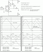
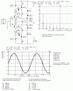
I used two input signals and plotted the power dissipation in the components. As a first input signal a triangle was used with a +26V/-26V amplitude (52Vpp) to show the dissipation at any output level. Only resistive loading at this moment; maybe interesting to see what happens with reactive loading. It is clear that the resistor takes part of the dissipation. The total dissipation in the top half (R1, Q1,2) is about equal to the dissipation in the bottom hald (Q3). On average the resistor takes most of the dissipation.
You can also see that the resistor takes the power especially at small signal levels. For audio this is interesting, as the average audio level is normally quite small. Therefore I repeated some simulations with a 10Vpp sinewave (+5V/-5V). Now, 70% of the power is dissipated in the resistor, 17% in Q1 and 13% in Q2. The top right waveform shows the output voltage and the collector voltage of Q1; the switching of Q2 is clearly visible .
Steven
Thank you for your interest and remarks. I would like to address them in order.
I think it depends on the kind of resistor. Enamelled wirewound resistors may get as hot as 450°C, more than any transistor. SeePRR said:... You can't run resistors really-really hot and expect long life either...
http://www.vishay.com/docs/50008/rwm.pdf. Incandescent lamps even more.
I don't think so. I actually added a resistor in series with the load, just on the other site of the output transistor.PRR said:...What you have really done is added a couple of power resistors in parallel with the load...
You are right, I was wrongPRR said:... I can't see a way it won't switch under any condition...
If you can show and defend a set of values that does not switch, I'll be very surprised.
. I just had half of the circuit in mind and did not look at the negative output current carefully. I was too quick posting the idea and did not do any calculations or simulations (also too busy last week). At the bottom I will show some simulations I have done just now, after your answer.No, as you can see from the simulations below the idle current can remain the same to stay in class A. No paradox here.PRR said:...If we take the situation where resistor drops essentially the whole idle power, the value of the resistors is about 16Ω for an 8Ω load, so the effective load is 16||16||8= 4Ω. To even stay Class A, we have to double the idle current just to drag these resistors around. But for the resistors to carry that new doubled idle current, they have to be 8Ω, total load 8||8||8= 2.6Ω, and now we have to triple idle current to stay Class A. I have not resolved this paradox, but I think all the solutions lead to higher total power dissipation, except the case where the resistor current is so small that it really does nothing...
Well, I was wrong regarding the switching of Q2. I think you are wrong regarding the dissipation reduction in the transistors. As an example I simulated the circuit in CircuitMaker for a 150Ω load. I just downloaded the student version that comes with a limited library, so I scaled down the currents to use some medium power transistors that were in the library.PRR said:... So I think all this does is add dummy resistors and heat. And I think it won't actually reduce transistor dissipation at all.
I don't mean to discourage you. I'd be real interested to see a system like this with reduction of transistor dissipation. I've certainly been wrong enough before. But I've run through a lot of such schemes, thinking I was "on to something", and eventually found the fallacy. (One recent one troubled me for 20 years.) My gut says this one won't work either. Prove me wrong.
I used two input signals and plotted the power dissipation in the components. As a first input signal a triangle was used with a +26V/-26V amplitude (52Vpp) to show the dissipation at any output level. Only resistive loading at this moment; maybe interesting to see what happens with reactive loading. It is clear that the resistor takes part of the dissipation. The total dissipation in the top half (R1, Q1,2) is about equal to the dissipation in the bottom hald (Q3). On average the resistor takes most of the dissipation.
You can also see that the resistor takes the power especially at small signal levels. For audio this is interesting, as the average audio level is normally quite small. Therefore I repeated some simulations with a 10Vpp sinewave (+5V/-5V). Now, 70% of the power is dissipated in the resistor, 17% in Q1 and 13% in Q2. The top right waveform shows the output voltage and the collector voltage of Q1; the switching of Q2 is clearly visible
. Steven
Attachments
Don't try to stick that one on me!john curl said:Old as the hills. ;-) Has been tried before, maybe patented by Nelson Pass.
Wow. Good presentation. At first glance, seems far better than I expected. Much to think about. I may brood on it for days and come back with more. But tonight:
> resistors may get as hot as 450°C
Sure, or more. Pull the Nichrome out of a room heater and run it red hot. If you are looking for size, though, you have to allow room for that heat to spread-out before it hits your fingers, the paint on your finger-guard, or the varnished shelf above it. A very high temperature dissipator can be smaller than the ones we use for transistors, but not a lot smaller, not in a home.
Yes, a hank of Nichrome or power resistor is cheaper than the same watts in Al extrusion at Si temperatures, possibly far cheaper.
We agree that, in any plausable configuration, it switches. It is just another class B amplifier plus an class A buffer. While the class A amp will isolate the class B spikes from the output a lot, the C-E voltage on the class A transistor goes through some sharp kinks that will tend to bleed-through, and the class B goes in and out of cutoff at small signal levels which, as you note, are critical in speech/music reproduction. On one hand we can dismiss this as "just a quality issue", but since the only reason to do class A these days IS quality, we have to ask if all this class B switching is worth the hoped-for smaller heatsink.
I'm wondering how far from class A this is. I'd like to see the current in Q1: does it sweep a sine or is it all kinky? (I agree that the graph is cluttered enough already). The way Q2 is kicking in and out is going to need a very fast Q2, or it will stay cut-off for many microseconds while Q1 is needing more voltage and current.
I am still impressed at that simulator. In mine, I'd have to set up a lot more gimmickry to get an average dissipation. And setting up anything takes time, something that is always in short supply. So while I'd like to see a different simulation (actually two simulations: Conventional and Steven's), I understand that may not happen.
OK, big objection to your simulation: you did not model both halves as "Steven's Amp" topology. Yes, I still believe those resistors are in parallel with the load, most obviously on the "other" side of the swing. The top resistor increases dissipation in the bottom transistor. So your half/half simulation is unfair: the top transistors are not driving a 300Ω resistor in the bottom, and the bottom transistor is sucking current from the top 300Ω resistor which it would not be doing in a "conventional" amplifier. You can't treat the two halves of a push-pull amplifier as separate, unless you run pure class B with complete switch-over at the zero crossing.
As evidence: why is Q1's dissipation increasing when the output swings negative and we would expect the top-half's dissipation to decrease?
Get both 300Ω resistors in there, and I think you will find transistor disspation as high or higher than a simple class A design.
Small niggles:
That top half can not swing higher than about 25V because of the 5V drop. Using a floating battery, when the ouput hits +25.6V, Q2's C-B junction will forward-bias and clamp the output. A diode in Q2's collector does not solve the problem even if we assume the floating battery can supply the load through Q2's B-E junction: Q1 can't deliver the current to pull-up the bottom of the battery and supply its own collector voltage. In practice, Vs1 would probably be a Zener fed from V+ through a current source, so the base of Q2 could not reach +30V and the output could not reach +25V. Yes, we could use less than 5V bias here, but we still need enough to keep Q1 working, so there will always be wasted voltage.
The conventional stage does not have this wasted voltage, so it could be run at a lower supply voltage. Not 5V less, because you do have the R3 drop to contend with. For a fair comparison, the Conventional and Steven's topologies need different supply voltages for equal clipping level, and a fair comparison must test that way.
Since it will only swing up to about 25V, with 150Ω load the peak current is 167mA and the idle current should be 88mA, not 100mA. This is unfair to the conventional side.
BTW: I doubt that 1V drop on the emitter resistors is optimum, 30mV has merit. But it sure is easier to set-up a simulation (or a real amp) without having to hand-trim bias.
Personally, I like to see the dissipation at zero power and at full sine power. No, full-sine is not normal for speech/music, but it is the "usual" way to compare amplifiers. In straight-A operation, dissipation is lowest at full-sine, in straight-B it is high at full sine. In B diss is actually highest at half-voltage, another point to check. For loudest un-clipped speech/music, quarter-voltage (1/16th power) is a nice test point.
Anyhow, big class A is easy. Bolt your trannies to a heavy copper box. Get an "ice maker kit": a thing that taps a water-pipe and a length of plastic tubing. Flow cold water through the copper box and to a drain or out the window. You can dump a lot of heat with a small stream of water. In home use, the operating costs (electric and water) will not be large unless you leave it on all the time.
Nelson Pass has designed an amp or two, including one with lightbulbs I believe, so I'd like to hear his off-the-cuff thoughts.
PRR said:
...OK, big objection to your simulation: you did not model both halves as "Steven's Amp" topology. Yes, I still believe those resistors are in parallel with the load, most obviously on the "other" side of the swing. The top resistor increases dissipation in the bottom transistor. So your half/half simulation is unfair: the top transistors are not driving a 300Ω resistor in the bottom, and the bottom transistor is sucking current from the top 300Ω resistor which it would not be doing in a "conventional" amplifier. You can't treat the two halves of a push-pull amplifier as separate, unless you run pure class B with complete switch-over at the zero crossing.
As evidence: why is Q1's dissipation increasing when the output swings negative and we would expect the top-half's dissipation to decrease?
Just a quick answer, since I'm time limited at the moment. I hope to show you some more simulations soon.
Actually, I did do the simulations with both halfs identical with resistor, with the same results. I just changed the bottom part afterwards with a conventional output half to be able to plot both waveforms in the same graph for comparison.
For the evidence question: If the output swings negative the dissipation in the top half indeed decreases, but that dissipation is built up out of the dissipations in Q1, 2 and R1. As the dissipation in R1 decreases rapidly, the dissipation in Q1 can increase although the sum still decreases. When the output voltage swings negative, the current through Q1 decreases and the voltage across Q1 will increase faster than normal, partly because the emitter goes down (negative swing) and partly because the collector goes up (less current through R1). This combination of current decrease and non proportional voltage increase causes a power increase.
That's for the moment. I will come back on this.
Steven
More simulations
The 30mV you mention is a nice value for a class AB stage. For class A it can be more, without problem, because we have less problems with changes in transconductance. For class AB with the gm-doubling phenomenon a value of kT/q is about right.
Some dissipation values:
Zero power: Q1 323mW, Q2 254mW, R1 2193mW (2770mW total)
25% sine: Q1 525mW, Q2 396mW, R1 1781mW (2702mW total)
Full sine: Q1 688mW, Q2 375mW, R1 613mW (1676mW total)
Other half show approx the same values; there is a small offset due to unequal NPN and PNP.
Steven
I agree with you. I never said it was the non plus ultra, but just an idea that popped up. Maybe it's worthless, maybe it can be improved and will give nice results in the end. It is not yet out of my mind.PRR said:...On one hand we can dismiss this as "just a quality issue", but since the only reason to do class A these days IS quality, we have to ask if all this class B switching is worth the hoped-for smaller heatsink.
The shape of the current through Q1 cannot be kinky for a sine wave input and output. It is the only (positive) path for the current to the load and the output stage is still class A. The current through R1 and Q2 will be kinky but add up to a nice sine wave.PRR said:I'm wondering how far from class A this is. I'd like to see the current in Q1: does it sweep a sine or is it all kinky? (I agree that the graph is cluttered enough already). The way Q2 is kicking in and out is going to need a very fast Q2, or it will stay cut-off for many microseconds while Q1 is needing more voltage and current.
[/B]
Average dissipation in CircuitMaker is easy; just click the probe-tool on a device. Below I will have a few more simulations.PRR said:I am still impressed at that simulator. In mine, I'd have to set up a lot more gimmickry to get an average dissipation. And setting up anything takes time, something that is always in short supply. So while I'd like to see a different simulation (actually two simulations: Conventional and Steven's), I understand that may not happen.
[/B]
Please see the new simulations below, with both halves as "My Amp".PRR said:OK, big objection to your simulation: you did not model both halves as "Steven's Amp" topology. Yes, I still believe those resistors are in parallel with the load, most obviously on the "other" side of the swing. The top resistor increases dissipation in the bottom transistor. So your half/half simulation is unfair: the top transistors are not driving a 300Ω resistor in the bottom, and the bottom transistor is sucking current from the top 300Ω resistor which it would not be doing in a "conventional" amplifier. You can't treat the two halves of a push-pull amplifier as separate, unless you run pure class B with complete switch-over at the zero crossing.
[/B]
I agree on the loss of some headroom because of the cascoding. Maybe a PNP switch (for the top half; NPN for the bottom half) in parallel to R1 that gets in if required would solve that problem mostly, but at the expense of a Vc-jump on the class A transistor.PRR said:That top half can not swing higher than about 25V because of the 5V drop. Using a floating battery, when the ouput hits +25.6V, Q2's C-B junction will forward-bias and clamp the output. A diode in Q2's collector does not solve the problem even if we assume the floating battery can supply the load through Q2's B-E junction: Q1 can't deliver the current to pull-up the bottom of the battery and supply its own collector voltage. In practice, Vs1 would probably be a Zener fed from V+ through a current source, so the base of Q2 could not reach +30V and the output could not reach +25V. Yes, we could use less than 5V bias here, but we still need enough to keep Q1 working, so there will always be wasted voltage.
[/B]
It is unfair to my circuit too. I could have decreased the idle current for this 150Ω load and 25V swing. A conventional circuit would give >25V, but then we're back on the previous issue of less headroom.PRR said:Since it will only swing up to about 25V, with 150Ω load the peak current is 167mA and the idle current should be 88mA, not 100mA. This is unfair to the conventional side.
[/B]
Yes, 1V drop on the emitter resistor was just for the sake of simplicity. No thinking about biasing.PRR said:BTW: I doubt that 1V drop on the emitter resistors is optimum, 30mV has merit. But it sure is easier to set-up a simulation (or a real amp) without having to hand-trim bias.
[/B]
The 30mV you mention is a nice value for a class AB stage. For class A it can be more, without problem, because we have less problems with changes in transconductance. For class AB with the gm-doubling phenomenon a value of kT/q is about right.
New simulation attached. At zero power not much to see, so no graphs. Top graph shows 25% voltage drive, then full sine, and finally the relevant currents that show still class A behaviour for the output transistors.PRR said:Personally, I like to see the dissipation at zero power and at full sine power. No, full-sine is not normal for speech/music, but it is the "usual" way to compare amplifiers. In straight-A operation, dissipation is lowest at full-sine, in straight-B it is high at full sine. In B diss is actually highest at half-voltage, another point to check. For loudest un-clipped speech/music, quarter-voltage (1/16th power) is a nice test point.
[/B]
Some dissipation values:
Zero power: Q1 323mW, Q2 254mW, R1 2193mW (2770mW total)
25% sine: Q1 525mW, Q2 396mW, R1 1781mW (2702mW total)
Full sine: Q1 688mW, Q2 375mW, R1 613mW (1676mW total)
Other half show approx the same values; there is a small offset due to unequal NPN and PNP.
Steven
Attachments
me> so the effective load is 16||16||8= 4Ω
I'm a dummy. While something has to drag the resistors around, the Class A stage doesn't have to. The effective load on the class A stage stays 8Ω (or 150Ω in Steven's simulations).
I have also been dumb about something else. I've ASSumed that the emitter of the booster transistors tracks 4.3V from the output. When the boosters are sourcing current, this is true. But when not sourcing current.... I'm a dummy. The emitters reverse-bias and can't track.
However.
Your simulator is lying. Put a differential voltage probe across the B-E junction of a booster transistor. Over one half of the wave it will be +0.7V as expected. On the other half, the B-E junction reverse-biases. Looking at Q2 (top booster), when the output sings to -25V, Q2's Base is at -20V. At this moment, the simulator shows R1's current as about 20mA. 300Ω*20mA= 6V drop from the +30V rail= +24V. There is 44 volts of reverse bias on Q2's B-E junction. This is outside rating, and more important: nearly any BJT will break-down at 7V reverse bias on the B-E junction. (It makes a great Zener.) Therefore Q2's Emitter must be at -13V, R1 has 43V across it, its current is 143mA not 20mA.
Check me. Aren't the boosters' B-E junctions getting a large reverse bias? And assuming they really Zener at 7V, won't that suck current from the resistors? Obviously your models (most transistor models) are not modeling the 7 volt reverse breakdown. Yet nearly all real transistors DO break-down. To model this, you may need a 6V-7V Zener across the B-E junction (and another diode to block the Zener's forward-bias conduction). When you do that, I think you will see very bent current waves in the "Class A" buffer transistors. Also higher dissipation in the resistors, which you may not mind.
This is "only a device spec", not a theoretical flaw. We could just add a 1N1004 diode in series with the emitter and fix it. We could, in theory, get transistors with high B-E breakdown (though probably low Beta, and aside from a few old small parts. I have not seen a symmetrical BJT in decades). Yes, a MOSFET is different, though I think you will just put so much reverse charge on the Gate-Channel capacitor that you'll have a helluva time getting it to switch-on again in time to catch the buffer before it runs out of resistor current. Also most practical MOSFETs have Gate protection diodes that will limit similarly, just at 20V+ instead of 7V.
Overall: I think this works as a low-voltage Class A buffer with a Class C booster, a perfectly practical design. The resistors DO dissipate the Class A idle heat, up to several volts output. At low powers, it really does look better than a simple Class A design. That is clever.
However the switching in the booster transistors is pretty extreme. At one end they pass full load current, they idle hard-off, and at the other end of the swing they (or their protection diodes) are in deep reverse bias. I have not made much study of Class G stages to know if this is worse than usual for such topologies. I suspect that getting the C stage to work without trashing-up the output is difficult. And you know a good AB stage gives excellent performance without the heat or the complication.
Hi PRR,
While doing the simulations, I also noticed that the Qeb zener was not acting. I mentioned this zener already in my first post, but at that moment I was still thinking this would be an issue for class AB only. Now I know it is also an issue for class A. As you wrote, the zener action can be prohibited easily by a power diode in the emitter of Q2 (or a small signal diode in its base), so I did not pay much attention to the fact that the transistor model did not incorporate the zener.
I agree with you that the switching of the booster transistors contradicts the original motivation for class A, even if the output transistors are isolating this switching. An additional cascode between Q1 and R1/Q2 would improve that isolation a lot, but would also consume some headroom (again).
This evening I got an idea on how to avoid the switching of Q2 including the absence of zener problems and still have the advantage of R1-dissipation. But before posting it, it may be wiser to do at least a small simulation. It uses only very few additional components.
Steven
While doing the simulations, I also noticed that the Qeb zener was not acting. I mentioned this zener already in my first post, but at that moment I was still thinking this would be an issue for class AB only. Now I know it is also an issue for class A. As you wrote, the zener action can be prohibited easily by a power diode in the emitter of Q2 (or a small signal diode in its base), so I did not pay much attention to the fact that the transistor model did not incorporate the zener.
I agree with you that the switching of the booster transistors contradicts the original motivation for class A, even if the output transistors are isolating this switching. An additional cascode between Q1 and R1/Q2 would improve that isolation a lot, but would also consume some headroom (again).
This evening I got an idea
on how to avoid the switching of Q2 including the absence of zener problems and still have the advantage of R1-dissipation. But before posting it, it may be wiser to do at least a small simulation. It uses only very few additional components.Steven
Steven said:This evening I got an idea
Well, I did the simulation this evening and it works (in the simulator).
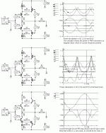
In the picture below you can see a possible solution to avoid that Q2 is switching. Only the top half is adapted, the bottom half is still conventional for comparison. Keeping Q2 conducting is done by adding a switch (Q5) in series with R1. If the current through Q1 is getting smaller because of a negative output voltage, the current through R1 is also getting smaller and the voltage drop over R1 decreases. But before Q2 can get reverse biased the current through Q2 will decrease to a value that cannot keep Q5 conducting via R6. The current through Q5 will go down, just as the current through R1. Since the amplifier is still biased in class A there must be a current through Q1 and that will be delivered by Q2 and R6. This keeps Q2 conducting and not switching off. The voltage on the collector of Q1 now nicely follows the output voltage with some offset, keeping the dissipation in Q1 low and its Vce stable. Most of the dissipation of the top half is in R1 (around 70% for small signals).
D1 and D2 are a Baker clamp to keep Q5 from going into saturation, as that would degrade high frequency performance.
The graphs show performance at 5Vp sine and 25Vp sine, indicating the voltages on A, B and C, and the power dissipation in the transistors and R1. For some stupid reason the simulator shows the dissipation in Q5 as a negative value. That should be positive, of course.
Although all this trickery wastes some headroom of the circuit, I still think it has potential. The transistors run considerably cooler and the most important transistor (audio wise) Q1 has an easy job, having a tracking cascode for linearity and limited dissipation.
Steven
Attachments
Cool class A (at least the transistors)
My previous post dropped from the first page, so it is about time to add a few things. I hope to get some remarks from you audio guru's and circuitry wizards.
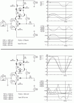
I think I have improved the idea that I started in this threat. I improved the tracking cascode, by sensing the emitter of the output transistors. Being independent now from the voltage drop across the emitter resistor, the Vce of the output emitter follower can be made smaller and better kept constant. The power dissipation in the output transistor is now really small in comparison to the power in the load, while still running in pure class A. With almost 54Vpp output voltage across 150 Ohm, the output power is 2.3W while the dissipation in Q1 and Q3 is only 50mW. The dissipation moved to Q2, Q5 and R1 (and Q4, Q7, R7 for the other half). But these have no problems with thermal stability because of idle current changes. The idle current is determined only by the the bias voltage and Q1, Q3, R1, R4.
Interesting is the case with no signal, because that will be the situation for most of the time. Average audio output is only very small. Now the dissipation is almost all in R1 (and R7), namely 2.7W, while Q1 and Q3 still dissipate only 57mW!
Distortion at full power is very low (at least that is what the simulator tells, but that is only a simulator): 0.015% and that is still open loop. No crossover distortion, of course. Since it is push pull the even harmonics are a little lower than the odd. At the emitters of Q1 and Q3 this is still the other way around (even bigger than odd), but the even harmonics cancel at the output (but not perfectly).
This is all still a mental exercise, nothing has been built yet. Also this is not very interesting at the current levels used for the simulation. For real power amplifiers it makes more sense, where the cost of some small signal parts and a few big resistors outweigh the cost of big heatsinks. The tracking cascode improves linearity anyway.
Another thing about this circuit is that it is able to deliver more current than would be available in class A. If necessary because of a lower speaker impedance it will just shift into class AB, and deliver the required current.
Your comments please... (PRR?)
Steven
My previous post dropped from the first page, so it is about time to add a few things. I hope to get some remarks from you audio guru's and circuitry wizards.
I think I have improved the idea that I started in this threat. I improved the tracking cascode, by sensing the emitter of the output transistors. Being independent now from the voltage drop across the emitter resistor, the Vce of the output emitter follower can be made smaller and better kept constant. The power dissipation in the output transistor is now really small in comparison to the power in the load, while still running in pure class A. With almost 54Vpp output voltage across 150 Ohm, the output power is 2.3W while the dissipation in Q1 and Q3 is only 50mW. The dissipation moved to Q2, Q5 and R1 (and Q4, Q7, R7 for the other half). But these have no problems with thermal stability because of idle current changes. The idle current is determined only by the the bias voltage and Q1, Q3, R1, R4.
Interesting is the case with no signal, because that will be the situation for most of the time. Average audio output is only very small. Now the dissipation is almost all in R1 (and R7), namely 2.7W, while Q1 and Q3 still dissipate only 57mW!
Distortion at full power is very low (at least that is what the simulator tells, but that is only a simulator): 0.015% and that is still open loop. No crossover distortion, of course. Since it is push pull the even harmonics are a little lower than the odd. At the emitters of Q1 and Q3 this is still the other way around (even bigger than odd), but the even harmonics cancel at the output (but not perfectly).
This is all still a mental exercise, nothing has been built yet. Also this is not very interesting at the current levels used for the simulation. For real power amplifiers it makes more sense, where the cost of some small signal parts and a few big resistors outweigh the cost of big heatsinks. The tracking cascode improves linearity anyway.
Another thing about this circuit is that it is able to deliver more current than would be available in class A. If necessary because of a lower speaker impedance it will just shift into class AB, and deliver the required current.
Your comments please... (PRR?)
Steven
Attachments
Interesting. Mind-blowing complicated; I don't think my skills can take it all in. It certainly does "switch its butt off", though it all has to pass through Q1 so maybe the switching is not audible. Stacked or floating supplies could get similar result (full Class A without full heat) but add cost and their own complication.
Maybe someone else will have intelligent comments.
Maybe someone else will have intelligent comments.
- Status
- This old topic is closed. If you want to reopen this topic, contact a moderator using the "Report Post" button.
- Home
- Amplifiers
- Solid State
- Spreading the heat in class A