Just looking at diodes. The diode in the model is a MUR460, a 600V 4A If, 1.8A Irr device, however they don't give the Qrr value, the switching time is 75nS. (data sheet: datasheet). The assumption here is more current for longer = higher power.
This may be a better option: datasheet it's a 600V 3A forward but a 1.2A Irr, Qrr=17.5nC and the recovery time is around 9nS. It copes with 32W and can be heatsink mounted.
So 0.5*1.75e-8*200^2 = 0.00035 joules per switching event.
78000*0.00035 = 27.3W of reverse power.
This may be a better option: datasheet it's a 600V 3A forward but a 1.2A Irr, Qrr=17.5nC and the recovery time is around 9nS. It copes with 32W and can be heatsink mounted.
So 0.5*1.75e-8*200^2 = 0.00035 joules per switching event.
78000*0.00035 = 27.3W of reverse power.
Last edited:
Interesting using a 3750 for efficient Kilovolt charging: http://etd.fcla.edu/CF/CFE0002899/Islas_Michael_E_200912_MS.pdf
3750 is the 3751 without the regulation feedback.
3750 is the 3751 without the regulation feedback.
I've been reading more heavily.
The minimum load is relatively easy to configure - selecting the feedback voltage divider to produce load to ground is the way that is done.
This brings me to current and specifically the Ipk and the Imin for regulation that is also quoted in the document. The Ipk on my case is 19A (given by a 5.5mOhm Rsense resistor).
The CSN pin internally is held between 11mV (min current) and 106mV (95% duty cycle) for the max current during regulation. Thus the Rsense provides working boundaries of the regulation current.
There's also Iload and the duty cycle current sensed. The 3751 has a 10% minimum Iload based on the peak. So in my case this is 19A/10 = 1.9A.
So now if the sensed current load detected using the FB voltage drop (I assume) then the key is how much primary current can we regulate between (ie 11mV and 106mV) without triggering the noisy charge mode for CSN:
0.011/0.0055 = 2A
0.160/0.0055 = 29A
So this is basically a minimum of 1.9A primary side or 190mA secondary side (1:10) to a max of 1.9A. That should be fine in terms of range as long as the load is 500mA. The interesting point is that 2.9A means the diode on the secondary side should be able to take at least 4A to give some overshoot room.
The question is how good is the regulation and how does that work?
Well the main comparator compares the FB with 1.22V. Using 6mF of capacitance helps this point about small signals " The feedback loop requires the output pole frequency to remain below 200Hz" as the output is subject to a 0.5Hz LPF which gives a -35dB at 200Hz.
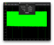
The average here is 177mA which may be causing an issue with the 190mA minimum.. RMS is 310mA which is less than I'd expect but the amp is running 447mA not full transient 3.16V input.
The minimum load is relatively easy to configure - selecting the feedback voltage divider to produce load to ground is the way that is done.
This brings me to current and specifically the Ipk and the Imin for regulation that is also quoted in the document. The Ipk on my case is 19A (given by a 5.5mOhm Rsense resistor).
The CSN pin internally is held between 11mV (min current) and 106mV (95% duty cycle) for the max current during regulation. Thus the Rsense provides working boundaries of the regulation current.
There's also Iload and the duty cycle current sensed. The 3751 has a 10% minimum Iload based on the peak. So in my case this is 19A/10 = 1.9A.
So now if the sensed current load detected using the FB voltage drop (I assume) then the key is how much primary current can we regulate between (ie 11mV and 106mV) without triggering the noisy charge mode for CSN:
0.011/0.0055 = 2A
0.160/0.0055 = 29A
So this is basically a minimum of 1.9A primary side or 190mA secondary side (1:10) to a max of 1.9A. That should be fine in terms of range as long as the load is 500mA. The interesting point is that 2.9A means the diode on the secondary side should be able to take at least 4A to give some overshoot room.
The question is how good is the regulation and how does that work?
Well the main comparator compares the FB with 1.22V. Using 6mF of capacitance helps this point about small signals " The feedback loop requires the output pole frequency to remain below 200Hz" as the output is subject to a 0.5Hz LPF which gives a -35dB at 200Hz.
The load must be constrained such that the output voltage ripple does not exceed the regulation range of the error amplifier within one clock period (approximately 6mV referred to the FB pin

The average here is 177mA which may be causing an issue with the 190mA minimum.. RMS is 310mA which is less than I'd expect but the amp is running 447mA not full transient 3.16V input.

Last edited:
So I'm just setting up up a bill of materials for this - I've decided to have a go myself first and I will attempt to make a 2 layer board with SMD using paste and a mask. I've studied the evaluation board 4 layer layout and a number of other implementations - both two layer.
I've started putting it in KiKad too but so far I've had to create footprint and symbol files for the 3751, the coil craft transform and some of the SMD aren't catered for - namely the current sense resistor.
I think it's possible to prototype this with a double sided board. It may not as performant as a multi-layer but it will be easier to make and debug. Initially I'll be using a small 450V cap and a power resistor as the load acting as a bleed resistor. It's using a single non-SMD mosfet that can be heatsink mounted at the side of board - the design takes that into account.
The main concern I have is the current and traces, calculations have 2.4mm minimum of 72um copper, that's even larger with 35um (1oz) and rises to 6.4mm with if I start using internal layers to transport current. Even with 1oz it may need some help.
The plan is to run a low current limited 12V prototype, check to ensure everything is working then switch up to 24V and ramp up the current and capacitance.
Last edited:
Don't forget when ordering resistors - most SMD resistors are rated for much lower voltages that you are aiming at.
That and if you need to use a shunt, get a through hole thick film TO220 SMD shunts may sound nice in theory, but are hard to solder in practice.
Yup, they use a Vishay WLS 1/4 watt in the eval board which is too low wattage. I was looking at replacing that with something based on 5.5mOhm * 50A^2 =1.3W (the transformer limits are 50A@12V or 25A@24V) but I was actually going to use a larger SMD wattage still at 7W given any spikes (TI recommend Imax+Ispike+20% so this should be enough).
My concern is making start noisy switch area larger with a TH sensing resistor vs the heat that it would generate, the derating that causes and so going for the larger sense resistor would provide more heat dissipation.
I'll have some shut eye, the have anther look.
I was doing some final checks and decided to look at the a couple of calculations for the transformer.
In short the transformer can't supply enough current in the pulse periods to support the power levels.
I couldn't put my finger on it until that point.
The transformer has a maximum power output with that chip of 136W which works out at 654mA at 200V, however at 70% efficiency that's actually 95W then when you start looking at the uH needed, that's where it breaks down.
The raw maths ignoring the switching periods mean that it would be absorbing 25A at 24V or 600W but only getting a small amount out. So when you look at the rates and the clock pulse lengths, that when it becomes obvious that the clock pulse with 24V can't cause enough current thus you end up not getting power to the output.
C'est la vie.. now back to the drawing board again..
So this looks very interesting: https://www.analog.com/media/en/technical-documentation/data-sheets/LTC7840.pdf
Dual boost capable of providing 240V 700mA from 12V when configured in cascade. No idea of the noise. Need to look at this more carefully. Certainly horrifically complex from a board layout, it has some interesting features - current limiting and soft start that keeps hiccup mode at bay until the caps are charged (needs modelling to check that).
Dual boost capable of providing 240V 700mA from 12V when configured in cascade. No idea of the noise. Need to look at this more carefully. Certainly horrifically complex from a board layout, it has some interesting features - current limiting and soft start that keeps hiccup mode at bay until the caps are charged (needs modelling to check that).
Last edited:
I've started looking at the LT version of v4lve lover's suggested UC3845, the LT1241 way way simpler. that particular chip does 50% duty max too. However the LT1242&3 in the series that do 100% duty cycle.
I have the current model setup with FB setup for 200V, with a 10A limit initially, so let's see what happens. I have noted once nice bit - you can make the system vary it's frequency too unlike the fixed 3751.
I have the current model setup with FB setup for 200V, with a 10A limit initially, so let's see what happens. I have noted once nice bit - you can make the system vary it's frequency too unlike the fixed 3751.
Interesting: https://www.ti.com/lit/an/slua101/slua101.pdf?ts=1615657994277
I thought the LT3751 LTSpice model was slow!
I thought the LT3751 LTSpice model was slow!
So the LT1241 (0-50% Duty cycle) and the LT1243 (50-98% duty cycle) with isolation through the coil craft 1:10 20A 24V, 50Khz doesn't seem to be able to drive well enough.
Keep in mind that the 24Vdc mean well medical PSUs are isolated and so any mains transients (lightning strikes etc) have to make it through that PSU first.
So keeping it super simple, a 24V non-isolated boost-converter with a single inductor seems to be an option.
The LT3473 has a maximum frequency of 1MHz and is tuneable using an RC combo. This also has the usual simple current limiting through a sense resistor (not kelvin type) plus a voltage feedback mechanism.
Compared to the LT3751, or at least the LTspice model, it seems noisy as hell - with careful noise control needed pretty much everywhere.
So I'm currently exploring (rather than creating my own PWM etc) if the LT1243 could be used to manage a non-isolated boost converter. Naturally there a voltage rise on the switch but the LT chip doesn't need a connection between the inductor and the switch.
So far it seems like a decent match. However I'm still modelling it. Naturally there's the concern with stability with >50% duty cycle.
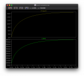
What is nice is that my favourite archaic trick of putting 5.1R+6mF between the diode and the load means that the feedback to the chip is smoothed. I'm still playing but at 120V 420mA at the moment although something has switched off the climb rate towards 200V so I'll need to investigate.
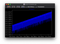
Here's a snapshot of the B+:
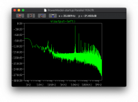
FFT across the whole model 400ms period.
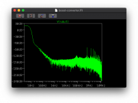
It's looking promising, this was simply the first run to try the idea so with some tuning this may be an option.
Keep in mind that the 24Vdc mean well medical PSUs are isolated and so any mains transients (lightning strikes etc) have to make it through that PSU first.
So keeping it super simple, a 24V non-isolated boost-converter with a single inductor seems to be an option.
The LT3473 has a maximum frequency of 1MHz and is tuneable using an RC combo. This also has the usual simple current limiting through a sense resistor (not kelvin type) plus a voltage feedback mechanism.
Compared to the LT3751, or at least the LTspice model, it seems noisy as hell - with careful noise control needed pretty much everywhere.
So I'm currently exploring (rather than creating my own PWM etc) if the LT1243 could be used to manage a non-isolated boost converter. Naturally there a voltage rise on the switch but the LT chip doesn't need a connection between the inductor and the switch.
So far it seems like a decent match. However I'm still modelling it. Naturally there's the concern with stability with >50% duty cycle.
What is nice is that my favourite archaic trick of putting 5.1R+6mF between the diode and the load means that the feedback to the chip is smoothed. I'm still playing but at 120V 420mA at the moment although something has switched off the climb rate towards 200V so I'll need to investigate.
Here's a snapshot of the B+:

FFT across the whole model 400ms period.

It's looking promising, this was simply the first run to try the idea so with some tuning this may be an option.
Last edited:
Hmm..
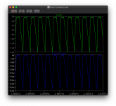
I noted an interesting cycle occurring, given it's now running at the 200V, almost like an idle rev-stop-rev-stop-.. when you look at the current across the diode.
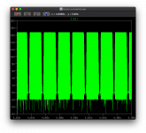
Looking at the output - this is obviously causing a slow oscillation, when you zoom in.. sure enough:
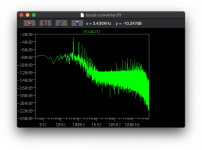
Looking at the oscillator RC.. hmm not here (although I can see a trace)..
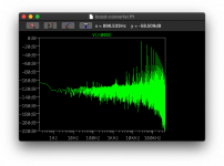
Looking at the gate output.. that's the source of the 50Hz noise..
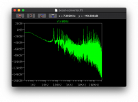
I suspect that the FB is causing the system duty cycle, so the system keeps the same frequency set by the RC but then duty cycles by cutting cycles out causing the revving idle.
This could be fixed - adjust the oscilator to produce less power per oscillation (ie increase the frequency which would make for smaller transfers), or reduce the current which would mean more on time to keep it from idling but that would be difficult to perform using a static system on a dynamic problem.
I'd removed the dynamic slope compensation to keep to simple to get the thing working - that could help, adjusting the slope based on current could work...
I noted an interesting cycle occurring, given it's now running at the 200V, almost like an idle rev-stop-rev-stop-.. when you look at the current across the diode.

Looking at the output - this is obviously causing a slow oscillation, when you zoom in.. sure enough:

Looking at the oscillator RC.. hmm not here (although I can see a trace)..

Looking at the gate output.. that's the source of the 50Hz noise..

I suspect that the FB is causing the system duty cycle, so the system keeps the same frequency set by the RC but then duty cycles by cutting cycles out causing the revving idle.
This could be fixed - adjust the oscilator to produce less power per oscillation (ie increase the frequency which would make for smaller transfers), or reduce the current which would mean more on time to keep it from idling but that would be difficult to perform using a static system on a dynamic problem.
I'd removed the dynamic slope compensation to keep to simple to get the thing working - that could help, adjusting the slope based on current could work...
A little low on the B+ but a tweak to the resistor of the RC oscillator control removed that - reducing the power a little to force it not to idle.
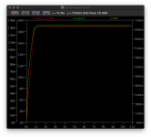
Not bad.
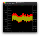
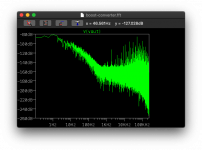
There's more tuning that could be done, but in reality you need the thing built before you can tune it. What is clear is that the getting the duty cycle to support the required performance is possible but there are some serious caveats with the LT1243 in terms of shaping and dynamically adjusting the amount of drive. The RC based control is adaptable but it's difficult to manage, especially for a dynamic load like an amp (Class A is perhaps better than AB in this respect).
I've been thinking of using small microcontroller and CPLD. I was thinking that a set of zener diodes could provide limit switching on/off for the CLPD (they don't have maths or ADC) and the CPLD then provides the required high rate for the PWD pulses give the duty rate given by the CPU. If the limit trigger is hit then the CPLD can immediately respond (ie stopping gate pulses) for example then the CPU can catch up.

Not bad.


There's more tuning that could be done, but in reality you need the thing built before you can tune it. What is clear is that the getting the duty cycle to support the required performance is possible but there are some serious caveats with the LT1243 in terms of shaping and dynamically adjusting the amount of drive. The RC based control is adaptable but it's difficult to manage, especially for a dynamic load like an amp (Class A is perhaps better than AB in this respect).
I've been thinking of using small microcontroller and CPLD. I was thinking that a set of zener diodes could provide limit switching on/off for the CLPD (they don't have maths or ADC) and the CPLD then provides the required high rate for the PWD pulses give the duty rate given by the CPU. If the limit trigger is hit then the CPLD can immediately respond (ie stopping gate pulses) for example then the CPU can catch up.
Last edited:
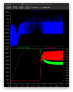
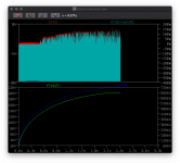
So this is the full amp model, 3 seconds in the negative bias is switched off, 5 seconds the mute is disabled.
The amp needs tuning but that's irrelevant at the moment - the B+ needs boost ing 20V to get the right 150V at the tubes. What I was interested in is the behaviour of the power supply input (blue) that would be connected to the 450W 24V MSP supply.
So there's the initial capacitor charge before 3 seconds. As the voltage gets close to 190V, the system starts blanking pulses to reduce power. Then at 3 seconds then all 12 triodes in the system are released from the 0V grid, 24V cathode (ie -24V grid) clamp and the system starts conducting. One ecc99 (red) shows this - this should run at 25mA ±30mA max signal once the B+ is corrected (due to additional filtering).
You can see the switch back to supplying power again as. The rough average of power draw at this point is 38W - ideally this should be about 45-50W to not drop below 10% power limit. One option is to simply reduce the PSU to a 300W and then alter the boost converter, limit the max current draw (sense resistor) and then have it always be above the 30W minimum it would be with that power supply.
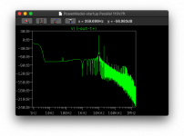
Just on the portion around the 5 second mark, the FFT shows a strong 10KHz this is the input 10KHz sine wave being amplified. I am concerned about the ~63Hz spike that could be from cycle skipping (the other channel is running a 30Hz input).
This brings me onto to what I was thinking about last night. The need for the system to maintain a cycle rate outside of the audio spectrum when in regulation mode (something that the LT3751 does automatically but the LT124x series does not).
The minimum duty cycle rate after skipping should be either 0 or 100Khz, additional cycles for additional power should the cause noise above 100Khz. The slope of the cycle should also be such that the additional noise and harmonics generated are above 100KHz. However the PSU needs to supply enough Q per pulse to maintain 50W. The system can then shape the pulse (sawtooth to square) and the number of pulses to focus on minimum noise created by other components. Current limit for primary side and voltage FB on the secondary. I could have noisy mode (ie max power start) and non-noisy mode along with a no-load mode (again safety first).
Those are my 'requirements' as such from a PWM controller.
Now I will setup the model to correct for the B+, and then there's a obvious point about improving the power shaping (ie the RC filter altering behaviour vs power) to maintain a 100KHz minimum period if possible.
Last edited:
So with some tweaks, it's doing 150V at the output tubes, with a tweak to the oscillator (low resistor meaning steeper charge rate thus more power per pulse) means it's drawing less power overall. It seems happy with the peaks pulling 130W, averaged it's probably 1/2 that.
This is running 447mV line input but it's a little quiet (original tuning was for 3.16 +20dBV transients without overloading the headphones). So I need todo another run with 3.16 to see how the PSU responds to large sustained transients (this causes the signal to max out the ecc99s so it'll be drawing it's maximum current regardless of tuning).
It's also not allowing the PSU to drop back and start skipping cycles which means the frequencies for noise are higher so less noise overall.
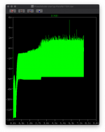
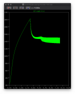
So this is looking like a 300W 24V 14A-rated PSU would be ample for running this.
This is running 447mV line input but it's a little quiet (original tuning was for 3.16 +20dBV transients without overloading the headphones). So I need todo another run with 3.16 to see how the PSU responds to large sustained transients (this causes the signal to max out the ecc99s so it'll be drawing it's maximum current regardless of tuning).
It's also not allowing the PSU to drop back and start skipping cycles which means the frequencies for noise are higher so less noise overall.


So this is looking like a 300W 24V 14A-rated PSU would be ample for running this.
- Home
- Amplifiers
- Power Supplies
- Tube use? 24->300V large cap charger with 300V 150mA reg
