A few members asked me to start a new thread for these two circuits. I made them while playing with the denoiser circuit presented in this thread. The denoising circuit was developed by Elvee and improved by Diego.
I applied the denoising circuit to two types of discrete regulators and it improved their performance by quite a bit. They both have a PSRR of more than -140dB depending of output voltage/current.
I also made some pcb designs for both, with and without a capacitance multiplier. Depending on your needs it can improve the PSRR to around -200dB.
Both circuits can be made with regular parts but for maximum performance certain BJTs should be used. Voltage reference can be either two LEDs in series, Zener or even LM329. PCBs have footprints for all of these. Out of all three options LEDs have the worst tempco but it's usable.
Voltage output range should be pretty wide and limited by capacitor voltage rating and transistors used. In simulation I managed to get 30V/4A output from both circuits but some modifications are required for mora than 1A current output.
For up to 30Vout you could use two LEDs in series but above this you should switch to Zeners. I tested with IR, red, yellow, orange and green LEDs and worked fine with either. I tested this for the Vref LEDs and also the CCS LED. I recommend using red LEDs, you can use the model in the LTSpice sim files so you can test your needed part values.
I built and measured both designs with earlier versions of the posted pcbs.
If you have questions about recommended part values for certain voltage/current output I will try to help.
I'll attach the pcb designs in the next post.
Attachments

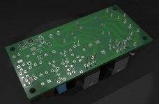
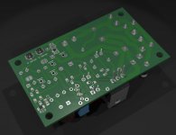
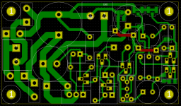
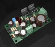
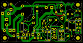
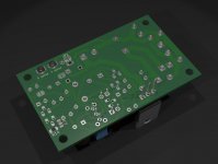
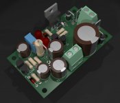
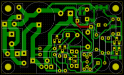
This is the pcb design for the first circuit. This pcb is single sided and can also be diy-ed. It requires two top links, but you don't have to do anything if you make the pcb at fab house, there are top traces.
You can use a potentiometer or simple resistors to set the output voltage. There's footprints for two 5mm LEDs in series, you can install a Zener between these footprints, and there's also a LM329 footprint.
JP1 should be soldered closed. JP2/JP3 jumpers are for sensing the noise at the output connector. There's footprints for u.fl connectors if you want to use coax for remote sensing. In case you want to use remote sensing you keep JP2/JP3 open. You can also use two normal wires, twisted together, for remote sensing. Just solder them on the signal pad of the u.fl connector.
The _cm files are the version with the extra capacitance multiplier which ads around -55dB to total PSRR.
Boards sizes are 37mm x 65mm for the normal one and 38mm x 80mm for the one with capacitance multiplier.
Attachments
Last edited:
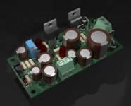
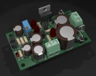
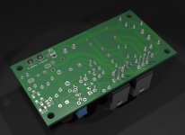
This is the second circuit pcb. It has the same Vref arrangement as the previous board. Same deal with jumpers.
There's a large resistor footprint, it can be used with a normal 0.4/0.6W resistor or a vertical mounted higher power one. This is in case you want to experiment with higher output current. With a smaller Vref you can move some of the heat (from pass transistor base current) into this resistor.
This board is also diy-able and requires a top side link. There's a top trace if you make it at fab house.
Board sizes are around 38mm x 64mm for the normal one and 38mm x 74mm for the one with capacitance multiplier.
I tested both designs with earlier versions of these pcbs. Measured both with a 60dB LNA and the PSRR is at -140dB or lower as that's right at my measuring gear limits.
Attachments
Forgot to mention, I built and measured both with a 60dB LNA on my PC's audio card.
Both circuits have at least -140dB PSRR, as that's right at the limits of my measuring setup.
The second circuit seems to perform good with many models of pass transistors. Even with MJE350. TIP32C had a bit worse performance by few dBs. Both of these showed worse performance in LTSpice than in reality. I have no MJE15033 at the moment to test with.
I tried with few different output caps and didn't seem to make any difference, seemed stable with any but I didn't try any extreme values, 100-330uF with 50-200mOhm ESR.
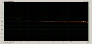
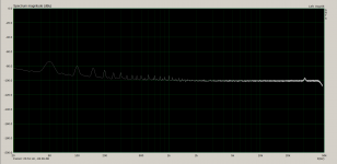
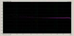
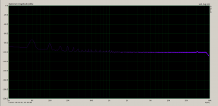
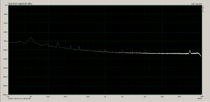
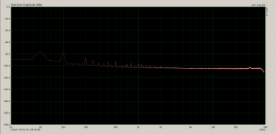
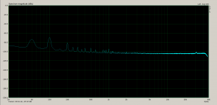
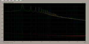
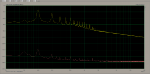
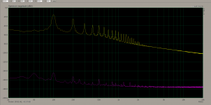
The attached pictures are measurements as follows:
1. first circuit with MJE15032. I've tried others and had worse results
2-4 second circuit with 2SB649, TIP32C and last one with MJE350. The TO-126 types are not compatible with these pcbs, I installed them backwards for testing only.
Measurements have some 50Hz parasitics and the 150Hz stuff is harmonic from the 50Hz, and those seem to depend on the position of the pcbs on my desk. I didn't use any kind of shielding while measuring.
The 0dB point is set at 1.3Vrms and when I measured the input ripple it was at around -1dB. So actual values are the ones on the left of the graph to which you add the -60dB from the LNA.
edit: picture 5 is the input ripple measured directly with the ADC on the pcb output, and picture 6 is the LNA connected to the pcb, pcb output shorted and turned off, for the lowest my LNA can sense. That signal at 30kHz+ is my modem's smps which is in the same power strip as the rest of the gear.
Both circuits have at least -140dB PSRR, as that's right at the limits of my measuring setup.
The second circuit seems to perform good with many models of pass transistors. Even with MJE350. TIP32C had a bit worse performance by few dBs. Both of these showed worse performance in LTSpice than in reality. I have no MJE15033 at the moment to test with.
I tried with few different output caps and didn't seem to make any difference, seemed stable with any but I didn't try any extreme values, 100-330uF with 50-200mOhm ESR.
The attached pictures are measurements as follows:
1. first circuit with MJE15032. I've tried others and had worse results
2-4 second circuit with 2SB649, TIP32C and last one with MJE350. The TO-126 types are not compatible with these pcbs, I installed them backwards for testing only.
Measurements have some 50Hz parasitics and the 150Hz stuff is harmonic from the 50Hz, and those seem to depend on the position of the pcbs on my desk. I didn't use any kind of shielding while measuring.
The 0dB point is set at 1.3Vrms and when I measured the input ripple it was at around -1dB. So actual values are the ones on the left of the graph to which you add the -60dB from the LNA.
edit: picture 5 is the input ripple measured directly with the ADC on the pcb output, and picture 6 is the LNA connected to the pcb, pcb output shorted and turned off, for the lowest my LNA can sense. That signal at 30kHz+ is my modem's smps which is in the same power strip as the rest of the gear.
Attachments
Last edited:
Yes, you just flip all polarities on diodes/capacitors and swap with complementary BJTs, on both PCBs. The LM329 footprint might be an issue but with a bit of tinkering you could make that work as well.
That is more of a secondary option, I made this with the intent of them being used with LEDs or Zeners for Vref.
edit: I'll build and measure the negative versions at some point when I find some time for this. LTSpice shows it should work.
That is more of a secondary option, I made this with the intent of them being used with LEDs or Zeners for Vref.
edit: I'll build and measure the negative versions at some point when I find some time for this. LTSpice shows it should work.
Last edited:
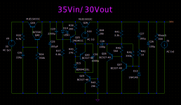
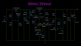
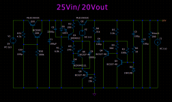
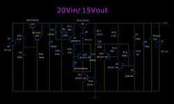
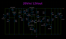
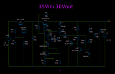
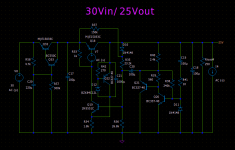
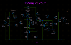
I made a set of recommended part values for different Vin/Vout conditions. All are for 100mA max output. I'll try and make another set for 1A output.
BJTs should be the ones in the sim for maximum performance. You can experiment with other models in sim. For best results I'd use a Zener as Vref.
In this post I'll attach the values for the first circuit, along with the sim file for all voltages.
A few notes about the requirements:
- if you don't want to use the capacitance multiplier on the pcb that includes it you can omit the parts and short C-E of the pass transistor.
- the 1000uF cap across Vref sees the Vref voltage + VBE of transistor so take that into account for its voltage rating.
- the 2200uF cap across the CCS LED sees only the LED Vdrop, so any 6.3V rated cap and up should work fine there.
- I've made the measurements with a random 5mm red LED for CCS. I'd use a red LED but you could experiment with IR as well, but the CCS resistor value changes.
- minimum Vdrop of the regulator itself is around 2.3V. min Vdrop for only the capacitance multiplier is around 1V, so take around 3.5Vdrop min for both. If you use the capacitance multiplier, on any of the output voltages for 100mA with input voltages in the sim you wouldn't really need a heatsink for any of the pass transistors.
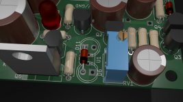
- the Zener can be installed as shown in the attached photo, between the LED footprints. The photo shows the orientation for the positive voltage output.
- Zener part numbers in the sim file are just an example. Their voltage rating matters, use tht types.
- the measurements I made are valid for these designs for PCBs, I can't guarantee them on other designs.
BJTs should be the ones in the sim for maximum performance. You can experiment with other models in sim. For best results I'd use a Zener as Vref.
In this post I'll attach the values for the first circuit, along with the sim file for all voltages.
A few notes about the requirements:
- if you don't want to use the capacitance multiplier on the pcb that includes it you can omit the parts and short C-E of the pass transistor.
- the 1000uF cap across Vref sees the Vref voltage + VBE of transistor so take that into account for its voltage rating.
- the 2200uF cap across the CCS LED sees only the LED Vdrop, so any 6.3V rated cap and up should work fine there.
- I've made the measurements with a random 5mm red LED for CCS. I'd use a red LED but you could experiment with IR as well, but the CCS resistor value changes.
- minimum Vdrop of the regulator itself is around 2.3V. min Vdrop for only the capacitance multiplier is around 1V, so take around 3.5Vdrop min for both. If you use the capacitance multiplier, on any of the output voltages for 100mA with input voltages in the sim you wouldn't really need a heatsink for any of the pass transistors.
- the Zener can be installed as shown in the attached photo, between the LED footprints. The photo shows the orientation for the positive voltage output.
- Zener part numbers in the sim file are just an example. Their voltage rating matters, use tht types.
- the measurements I made are valid for these designs for PCBs, I can't guarantee them on other designs.
Attachments
In this post I attached the recommended values for the second circuit for the same input/output voltages at 100mA.
Same deal with Vref bypass cap voltage rating, Zener can be installed the same across the LED footprints.
For this circuit Vdrop of the regulator itself is 0.6V minimum. The capacitance multiplier needs the same 1Vdrop. So around minimum 1.7Vdrop if you use both.
You can use two LEDs for Vref but that affects the ratio between the voltage setting resistors. Play with the sim file or just install them and adjust the potentiometer for the desired output voltage.
For the negative version I would personally make the same regulator and invert the output connections. This works with two secondaries. I don't think you can easily use the positive and negative versions of these PCBs with a center tapped transformer. Negative versions seem to have a bit worse performance so with two secondaries I'd use two positive regulators for both positive and negative rails.
I might try to make a dual PCB that shares the GND trace and has a voltage doubler on its input, so it could be used with a single secondary transformer.
Until I assemble and measure the negative versions for these PCBs I don't recommend trying it at the moment.
Attachments
I managed to test the negative versions. As I said before, all you have to do is to rotate 180 degrees all polarized parts, and replace all BJTs with their complementary.
The results seem to be very close to simulation. Again, on the negative version of the first circuit MJE350 seems to perform as good as 2SB649. Tried BD140 but was a few dB behind as performance, same as TIP32C. Since I have no MJE15033 I can't test with it, but I hope I'll get a few these days so I can test with it as well. It should measure better according to LTSpice.
The negative version of the second circuit measures few dB better than simulation. I only tried MJE15032.
All tests were done at 11.25Vout at around 90mA with a 150R load. I attached the LTSpice sim file with the exact values I used in my measurements.
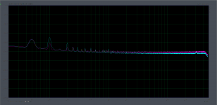
The attached measurements are as follows:
1. 1st circuit negative version with MJE350 which measures the same as 2SB649.
2. previous photo compared with positive version with MJE15032.
3. 2nd circuit negative version with MJE15032.
4. previous photo compared with the positive version with MJE350.
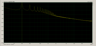
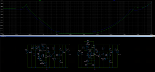
5. LTSpice sim PSRR for all 4 versions.
All measurements were done with 60dB LNA so add -60dB to the scale on the left. Since my 0dB is around the input ripple value the total PSRR value is the one on the scale with the -60dB from the LNA. I'll add the LNA gain to the ARTA graph in the future.
Below -140dB I don't think I can reliably see what's happening since there's 50/100Hz pickup and I don't have any shielding.
Also one curiosity, both negative versions seem to have a lower noisefloor than the positive versions. Might be due to pcb layout and reverse flow?
The results seem to be very close to simulation. Again, on the negative version of the first circuit MJE350 seems to perform as good as 2SB649. Tried BD140 but was a few dB behind as performance, same as TIP32C. Since I have no MJE15033 I can't test with it, but I hope I'll get a few these days so I can test with it as well. It should measure better according to LTSpice.
The negative version of the second circuit measures few dB better than simulation. I only tried MJE15032.
All tests were done at 11.25Vout at around 90mA with a 150R load. I attached the LTSpice sim file with the exact values I used in my measurements.
The attached measurements are as follows:
1. 1st circuit negative version with MJE350 which measures the same as 2SB649.
2. previous photo compared with positive version with MJE15032.
3. 2nd circuit negative version with MJE15032.
4. previous photo compared with the positive version with MJE350.
5. LTSpice sim PSRR for all 4 versions.
All measurements were done with 60dB LNA so add -60dB to the scale on the left. Since my 0dB is around the input ripple value the total PSRR value is the one on the scale with the -60dB from the LNA. I'll add the LNA gain to the ARTA graph in the future.
Below -140dB I don't think I can reliably see what's happening since there's 50/100Hz pickup and I don't have any shielding.
Also one curiosity, both negative versions seem to have a lower noisefloor than the positive versions. Might be due to pcb layout and reverse flow?
Attachments
I made a correction to the pcb designs. First, you should use BC327 for the Vref transistor, on both circuits. For the negative versions of each you'd use BC337. I tried 2N4403 in practical testing but BC327 works the same. The original pcb footprints are for BC327 pinout. If you want to use 2N4403 you have to rotate the BJT 180 degrees, and bend the middle pin the other way. You still have to bend that pin on all TO-92 parts as I used that type of footprint.
For the 1st circuit the CCS transistor has a footprint for BC560 type pinout but I recommend using 2N5401 for best performance. You can do the same, bend the middle pin the other way around and rotate the 2N5401 180 degrees.
For the 2nd circuit the 2N5551 transistor in the schematic also has a BC550 type footprint, and you'd have to rotate the 2N5551 as well, and I recommend using 2N5551 there for maximum performance.
As I said, you have to bend the middle pin anyway, just that you need to take into account to bend it the other way and rotate those BJTs. I attached the corrected project files for all versions, with and without capacitance multiplier for both circuits, and they have the correct footprints for 2N5551/2N5401 BJTs.
Also for capacitance multiplier the TO-92 transistor should be BC550 for best performance, the footprint is for BC337 but they are the same so nothing to do at this point, just use BC550 instead of the BC337 in the schematic.
1.zip is the first circuit without capacitance multiplier, 2.zip is the second circuit, and _cm to filename is for versions with capacitance multiplier.
Attachments
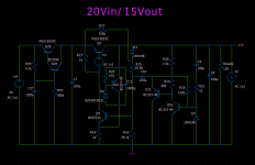
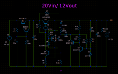
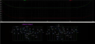
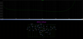
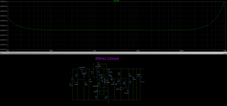
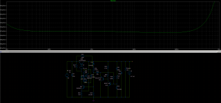
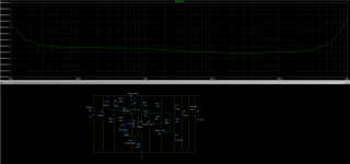
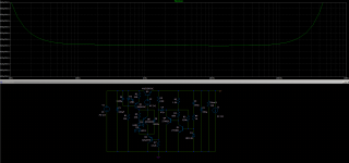
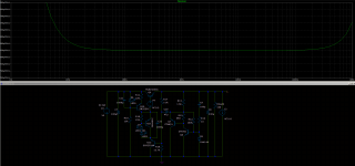
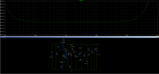
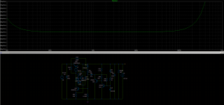
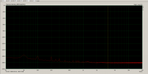
I also forgot to add the output impedance performance for both circuits. I attached the LTSpice sim results for both circuits for 12Vout at 100mA.
I can't measure it as I don't have the tools for that.
edit: also added .noise sim results for both circuits.
I can't measure it as I don't have the tools for that.
edit: also added .noise sim results for both circuits.
Attachments
Last edited:
The lower noisefloor in the last measurements for the negative versions of both circuits seems to be predicted in the LTSpice simulation as well. I think it's kind of close to the noise of the LNA itself.
Theoretically if you'd want the even lower noisefloor but can do with a bit less PSRR (maybe use with cap multi pcb) you could build two negative regulators if you have two secondaries, and use them for +/-. The first circuit seems to have a higher PSRR, but I'd have to confirm that once I get a MJE15033.
Theoretically if you'd want the even lower noisefloor but can do with a bit less PSRR (maybe use with cap multi pcb) you could build two negative regulators if you have two secondaries, and use them for +/-. The first circuit seems to have a higher PSRR, but I'd have to confirm that once I get a MJE15033.
Attachments
Last edited:
Also forgot one important aspect for all these 4 circuits. I just remembered that the denoiser seems to offer the lowest noise by using the ZTX951/ZTX851 combo. BC337/BC327 is a good low noise performer, but for best noise performance the ZTX pair should be used.
Simulation shows a reduction in noise such that it brings all 4 circuits in the same noise-value area, around 0.63nV/√Hz.
So using the ZTX pair for the denoiser circuit will offer the ultra-low noise to either of the 4 versions of regulator.
I might try to source these transistors but I think the regulators noise floor will be right about where the LNA noise floor is, with them installed. Combined with the capacitance multiplier it should offer extremely good performance for PSRR as well.
edit: using the ZTX pair also gives a 2-3dB boost to PSRR to all circuits. If you want to extract more PSRR from the 2nd circuit you can bypass D9 and D13 with a 330uF capacitor. It only sees the 0.6V or so across the diode so a 6.3V rating would be ok. This brings another 1.5dB or so, if you want to squeeze even more PSRR performance out of it (at 100Hz).
Attachments
Last edited:
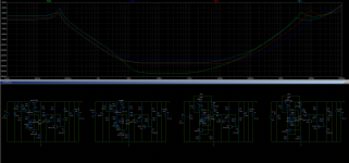
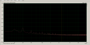
I remade the measurements for all 4 versions, both negative and positive versions for both circuits. I used 1300mA in ARTA as 0dB. Noise measurement for a 1k resistor results in 4.1nV/sqrtHz. Since now the LNA+ADC should show better results I decided to remake all measurements.
I'll first post the positive versions measurements for both circuits.
Output voltage was 11.4V at around 90-100mA. 1st circuit with MJE15032 and 2nd one with 2SB649 (MJE350 measures the same).
Attached pictures are as follows:
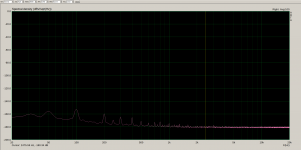
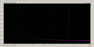
1. PSRR for positive first circuit. Results in -145.6dB for PSRR at 120Hz. LTSpice sim showed around -153dB at 100Hz. This circuit has the largest difference between simulation and measurement. I had to use a 220uF filter capacitor after bridge rectifier so I have a higher measurement dynamic range. The measurement is a low value and I'm not really sure if it's actually few dB lower, as at that level everything jumps a bit, 50Hz harmonic might also contribute to the 100Hz reading.
2. Noise measurement for the same circuit. At around 3.5kHz measured around 1.2nV/sqrtHz. LTSpice sim shows it should be 1.23nV/sqrtHz.
3. PSRR for positive second circuit. I used 220uF filter cap. Measures at -139.17dB and LTSpice sim shows -137.5dB.
4. Noise measurement for second circuit. Measurement shows 1.25nV/sqrtHz and LTSpice shows 1.23nV/sqrtHz.
I included archives with all measurements with cursor at point of values I posted.
I'll first post the positive versions measurements for both circuits.
Output voltage was 11.4V at around 90-100mA. 1st circuit with MJE15032 and 2nd one with 2SB649 (MJE350 measures the same).
Attached pictures are as follows:
1. PSRR for positive first circuit. Results in -145.6dB for PSRR at 120Hz. LTSpice sim showed around -153dB at 100Hz. This circuit has the largest difference between simulation and measurement. I had to use a 220uF filter capacitor after bridge rectifier so I have a higher measurement dynamic range. The measurement is a low value and I'm not really sure if it's actually few dB lower, as at that level everything jumps a bit, 50Hz harmonic might also contribute to the 100Hz reading.
2. Noise measurement for the same circuit. At around 3.5kHz measured around 1.2nV/sqrtHz. LTSpice sim shows it should be 1.23nV/sqrtHz.
3. PSRR for positive second circuit. I used 220uF filter cap. Measures at -139.17dB and LTSpice sim shows -137.5dB.
4. Noise measurement for second circuit. Measurement shows 1.25nV/sqrtHz and LTSpice shows 1.23nV/sqrtHz.
I included archives with all measurements with cursor at point of values I posted.
Attachments
Last edited:
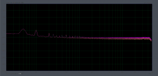
This post contains the measurements for negative voltage output versions of both circuits.
I used a total of 570uF (470uF+100uF) as filter capacitors on both boards, same 11.4Vout at 90-100mA.
Attached pictures are as follows:
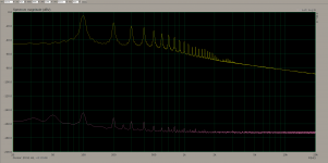
1. PSRR for the first circuit with 2SB649. Measured a total of 124.4dB at 100Hz. LTSpice sim showed 126.5dB at 100Hz.
2. Noise for the same circuit. Measured at 0.95nV/sqrtHz, LTSpice sim shows 0.92nV/sqrtHz.
3. PSRR for the second circuit with MJE15032. Measured a total of 129dB at 100Hz. LTSpice sim showed 134.4dB at 100Hz. Maybe the particular MJE15032 I used is not up to spec. It underperforms in both circuits.
4. Noise for the second circuit. Measured at 0.84nV/sqrtHz. LTspice sim shows 0.92nV/sqrtHz.
I will get the ZTX pair for denoiser in the future, also MJE15033 and I'll make another set of measurements.
edit: I didn't use the capacitance multiplier on any pcb, I removed the parts and shorted C-E of pass transistor footprint.
2nd edit: also the noise figure of my LNA came out at around 0.6nV/sqrtHz at 1kHz.
I used a total of 570uF (470uF+100uF) as filter capacitors on both boards, same 11.4Vout at 90-100mA.
Attached pictures are as follows:
1. PSRR for the first circuit with 2SB649. Measured a total of 124.4dB at 100Hz. LTSpice sim showed 126.5dB at 100Hz.
2. Noise for the same circuit. Measured at 0.95nV/sqrtHz, LTSpice sim shows 0.92nV/sqrtHz.
3. PSRR for the second circuit with MJE15032. Measured a total of 129dB at 100Hz. LTSpice sim showed 134.4dB at 100Hz. Maybe the particular MJE15032 I used is not up to spec. It underperforms in both circuits.
4. Noise for the second circuit. Measured at 0.84nV/sqrtHz. LTspice sim shows 0.92nV/sqrtHz.
I will get the ZTX pair for denoiser in the future, also MJE15033 and I'll make another set of measurements.
edit: I didn't use the capacitance multiplier on any pcb, I removed the parts and shorted C-E of pass transistor footprint.
2nd edit: also the noise figure of my LNA came out at around 0.6nV/sqrtHz at 1kHz.
Attachments
Last edited:
If you have questions about recommended part values for certain voltage/current output I will try to help.
Please, for 19Vout up to 4A current. I want to try to replace switch power supply that power my audio pc.
Regards
I recommend these pcb to be used to a max of 1.5A. And I'll have to release a set of values I'd recommend for this current output. I think it could be done for up to 30Vout, but I first need to check some things.
For the up to 4A output needs I don't recommend this pcb design. Some part footprints or even layout would have to be different, different bridge rectifier for the 4A of current.
For the 4A current output, also for a PC, I'd go with LM338+dienoiser. I thought about doing a pcb design for the full current output of the LM338 but that's something I didn't yet look into.
Also you have to keep in mind that replacing the SMPS with a linear regulator you'd have a good bit of efficiency loss. Also even if you put a clean supply for the PC, it usually has different buck/boost converters on its pcb, for the different rails that are usually needed.
So using a clean linear regulator as the main supply might solve some noise, but you'd still have some sources for HF noise in it.
- Home
- Amplifiers
- Power Supplies
- Discrete regulators with denoiser