About ripple rejection what BJT parameters are important.
In a topology, i am working on, Early voltage makes a lot of différence.
I understand there à feed through effect coming from the collector dynamic resistance related to Early voltage.
I think a good pass BJT should have hight VAF.
Low collector capacitance matters too.
What do you think.
In a topology, i am working on, Early voltage makes a lot of différence.
I understand there à feed through effect coming from the collector dynamic resistance related to Early voltage.
I think a good pass BJT should have hight VAF.
Low collector capacitance matters too.
What do you think.
Loose thaughts:
I think you are right--but a voltage regulator don't have to be as linear as a amplifier because the NFB is huge and the duty is to maintain a constant voltage which holds down the variation in base-collector-voltage so maybe speed (collector-base-capacitance) is more important.
On the other side, the NFB comes from the error amplification wich causes oscillation if too large.
In what way is the Early voltage important in your topology? Have you made some interesting measurements?
Last edited:
No measurement but interesting simulations that do show the Early voltage influence on PSRR.
Using the default LTSpice BJT I have an excellent Ripple Reduction at 100 Hz.
Then using an actual transistor model from the LTSpice library, I have a not so good PSRR. I found, that is because the default transistor VAR is infinity.
Actual transistors are more like VAR 100 V.
Tweaking VAR in the BJT model, I see that with VAR 500 V I do have better PSSR.
On DIYaudio, I saw
2SC6149 at VA 1600V.
2SA2223 at VA 540V
Those are 15A transistors.
2SA1381/2SC3503 at VA 700V/800V
Those are 100mA transistors.
Sure, a high loop gain is a great ripple reducer, but has you said, it taxes on stability.
The interest of a pass transistor high Early voltage is better ripple reduction without imparting stability.
Last edited:
Ripple rejection is the least of the problems and is easily fixed by having sufficient head room. The ability of the regulator to respond to high frequency load changes and transients is the pertinent issue. Thus, the regulator and pass elements must have a sufficiently high frequency response as well as being low noise.
An output capacitor is not the answer if/when load current demands exceed the ability of the regulator to "replenish" that capacitor at the same rate.
An output capacitor is not the answer if/when load current demands exceed the ability of the regulator to "replenish" that capacitor at the same rate.
I do not agree
More head room makes it easier but doesn't fix it.Ripple rejection is the least of the problems and is easily fixed by having sufficient head room.
This job is expected from appropriate bypass decouplings at the powered circuits. To count on the PSU to help means you have HF at the rails. I would hate rails and PSU acting as antennas spreading HF.The ability of the regulator to respond to high frequency load changes and transients is the pertinent issue. Thus, the regulator and pass elements must have a sufficiently high frequency response as well as being low noise.
1. Buy a different power transformer whose secondary voltage is about 3VAC greater than your current design
2. Build a cascade of two voltage regulators in series
3. Done!
2. Build a cascade of two voltage regulators in series
3. Done!
If you're building a voltage regulator at all, that means it's a line stage or active crossover or preamp or DAC or headphone amp etc; whatever it is, it draws far far less than 30 watts from the AC mains.
So you're buying a relatively small, relatively low VA transformer. The extra cost to purchase the 3VAC-higher-secondary-voltage transformer is: zero.
The first (upstream) voltage regulator acts as a wonderfully excellent cascode for the second (downstream) voltage regulator. So you don't need to worry about Early voltage very much.
The first voltage regulator reduces 2xfmains ripple by 40-70dB. This means the second voltage regulator can focus its design resources and parts budget upon other performance goals. Perhaps such as noise, output impedance, bandwidth, and stability.
Piling many stuff, I don't like much. Cap multiplier, Pre reg, Reg, Denoiser.
Along this line, one can also put massive capacitor reservoir. Each doubling of caps is garantied -6dB PSRR and no taxe on stability.
I like efficient solution cost wise.
I like one stage solution with not much reservoir cap.
Along this line, one can also put massive capacitor reservoir. Each doubling of caps is garantied -6dB PSRR and no taxe on stability.
I like efficient solution cost wise.
I like one stage solution with not much reservoir cap.
The end result of the Early effect is to modulate the Vbe as a function of Vce.
It will influence the PSRR of all topologies to some degree, but the effect is going to be maximal for buffered zeners or cap-multiplier topologies.
if the pass transistor is current-driven, the effect will be negligible.
Anyway, the most important parameter for a pass transistor is probably the SOA (for all conditions, including fault and transient): the rest can be dealt with relatively easily, but a transistor melt-down is more problematic

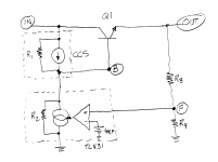
The topology I am working on:The end result of the Early effect is to modulate the Vbe as a function of Vce.
It will influence the PSRR of all topologies to some degree, but the effect is going to be maximal for buffered zeners or cap-multiplier topologies.
if the pass transistor is current-driven, the effect will be negligible.
The base of the pass transistor is driven by a node that has the cathode of a TL431 and a CCS.
The CCS brings current to the base of the pass transistor. The emitter of the pass transistor is at the regulated output.
The CCS is in // with the CB junction of the pass transistor.
This topology does exhibit a high dependence of the Early voltage into the 100Hz ripple reduction.
From VAF 100V to 500V a -14dB PSRR.
Last edited:
That makes sense if the current source is ideal or good enough to be regarded as ideal. When all other paths are negligibly small, the transfer from input ripple to output ripple will be determined by the ro of the transistor (I mean the resistance between collector and emitter in its small signal model) which is approximately inversely proportional to the Early voltage. Compared to the topologies Elvee wrote about, overall feedback via the TL431 will improve the PSRR, but the number of dB improvement when going from 100 V to 500 V will remain the same as long as the ro of the pass transistor is the main path to the output for 100 Hz ripple.
Early effect also changes the base width and should therefore change hFE, so I don't understand why it should be negligible when the transistor is current driven.
Early effect also changes the base width and should therefore change hFE, so I don't understand why it should be negligible when the transistor is current driven.
MarcelvdG. I fully agree with your analysis, well explained.
In my simulations, I use an ideal CCS with a shunt resistor to represent the dynamic resistance of a real CCS.
A CCS made of two BC857C in a ring configuration exhibits better than 3 MegOhm at voltages down to 1V, then drops sharply, 160K at 0.9V. This voltage is actually the pass transistor Vcb.
So, this real CCS is an ideal one considering the Early effect of the pass transistor.
jan.didden. I was confused about what drive is the pass transistor in my considered topology, current/voltage ? Open loop/closed loop ? Thanks to make it clear by a simple answer.
In most regs, the current source supplies the base of the pass transistor, and the opamp, through the feedback, draws away just enough current to maintain the output voltage.
That means that the base of the pass device 'looks into' the low impedance opamp output, and thus is voltage driven.
What that means is that in terms of parasitic capacitances, the pass device runs in grounded base.
Jan
That means that the base of the pass device 'looks into' the low impedance opamp output, and thus is voltage driven.
What that means is that in terms of parasitic capacitances, the pass device runs in grounded base.
Jan
The textbooks say that the output impedance of a voltage regulator is inversely proportional to (1+loopgain). Whether you believe the textbooks or not, is of course a personal matter.
Loop gain in the regulator below, is rather weak compared to modern alternatives. So the regulator below has rather higher output impedance compared to modern alternatives.
You can add one Zener diode and increase the loopgain by 2X, thus decreasing closed loop Zout by 2X.
You can add one bipolar transistor and decrease the openloop Zout by 75X, thus decreasing closed loop Zout by another factor of 75X.
But for SERIOUS improvements in closed loop Zout, you'll need significantly more gain than a one-stage error amplifier can provide. The Jung-Didden Super Regulator gets huge gain by including an opamp. Other voltage regulators get huge gain by using a (discrete transistor) two-stage or even three-stage error amplifier. And that's how they achieve extremely low closed loop Zout.
*authors of the book "The Art Of Electronics"
in the figure below, "R1" models the Norton equivalent resistance (a/k/a the output impedance, dI/dV) of the Constant Current Source. Similarly, "R2" models the output impedance (dI/dV) of the TL431. The single gain stage has its input connected to the feedback node "F" and its output connected to the base node "B". The series pass transistor acts as a load upon node "B" and this extra load reduces the gain. Because it's an emitter follower, the impedance looking into its base is approximately the resistance connected to the emitter (the output load driven by the regulator), times Beta.
_
Loop gain in the regulator below, is rather weak compared to modern alternatives. So the regulator below has rather higher output impedance compared to modern alternatives.
- Zout_closedloop = Zout_openloop / (1 + loopgain)
You can add one Zener diode and increase the loopgain by 2X, thus decreasing closed loop Zout by 2X.
You can add one bipolar transistor and decrease the openloop Zout by 75X, thus decreasing closed loop Zout by another factor of 75X.
But for SERIOUS improvements in closed loop Zout, you'll need significantly more gain than a one-stage error amplifier can provide. The Jung-Didden Super Regulator gets huge gain by including an opamp. Other voltage regulators get huge gain by using a (discrete transistor) two-stage or even three-stage error amplifier. And that's how they achieve extremely low closed loop Zout.
*authors of the book "The Art Of Electronics"
in the figure below, "R1" models the Norton equivalent resistance (a/k/a the output impedance, dI/dV) of the Constant Current Source. Similarly, "R2" models the output impedance (dI/dV) of the TL431. The single gain stage has its input connected to the feedback node "F" and its output connected to the base node "B". The series pass transistor acts as a load upon node "B" and this extra load reduces the gain. Because it's an emitter follower, the impedance looking into its base is approximately the resistance connected to the emitter (the output load driven by the regulator), times Beta.
_
Attachments
Last edited:
You are right, of course.Early effect also changes the base width and should therefore change hFE, so I don't understand why it should be negligible when the transistor is current driven.
To put some numbers to it: the TL431 has a typical transadmittance of about 5 S and a voltage gain of about 1000 up to 3 kHz when the voltage at node B exceeds 10 V, about 700 at lower voltages. So Rz ~= 200 ohm, open-loop Zout ~= 4 ohm guessing that beta ~= 49, loop gain ~= 1000 R4/(R3 + R4). With for example R3 = 5 R4, the closed-loop Zout is about 24 mohm, roughly 48 times the square resistance of 35 um thick copper.
Last edited:
24 milliohms finishes 3rd worst in the Linear Audio shootout:
LINK TO PDF
Better than Burson and SuperTeddy, worse than twelve others.
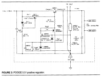
Embarrassingly, it's significantly worse than the POOGE all-discrete regulator: 3 milliohms on the graph. POOGE also has a single gain stage, driving a single NPN emitter follower pass transistor. It was published by Walt Jung in The Audio Amateur, Issue #1 of 1995. Schematic below.
Notice the protection diode across the base-emitter junction of low noise transitor Q855. That's not a rookie play. Notice the base stopper resistor Rr3. That's not a rookie play. And notice the little stunt which reduces the openloop output impedance by more than a factor of ten. Pretty good performance for a 25 year old circuit design using 4 discrete transistors.
_
LINK TO PDF
Better than Burson and SuperTeddy, worse than twelve others.
Embarrassingly, it's significantly worse than the POOGE all-discrete regulator: 3 milliohms on the graph. POOGE also has a single gain stage, driving a single NPN emitter follower pass transistor. It was published by Walt Jung in The Audio Amateur, Issue #1 of 1995. Schematic below.
Notice the protection diode across the base-emitter junction of low noise transitor Q855. That's not a rookie play. Notice the base stopper resistor Rr3. That's not a rookie play. And notice the little stunt which reduces the openloop output impedance by more than a factor of ten. Pretty good performance for a 25 year old circuit design using 4 discrete transistors.
_
Attachments
Last edited:
- Status
- This old topic is closed. If you want to reopen this topic, contact a moderator using the "Report Post" button.
- Home
- Amplifiers
- Power Supplies
- What makes a good pass transistor in a serie regulator