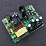
I've got three 500W +/-55V SMPS's (first attachment) that I bought from Aliexpress and eBay, two of which have faultlessly powered my 7-channel home theater power amplifier (based on LJM's L15D IRS2092 class-D modules), for more than three years now.
However, this SMPS doesn't have any effective short circuit protection, and I stupidly managed to blow up one of them by accidentally connecting it to a short circuit. That's why I've got three now - I had to buy a replacement, but I'd still like to have a go repairing this one.
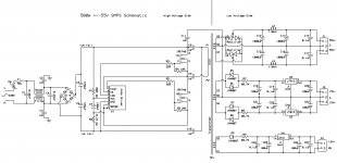
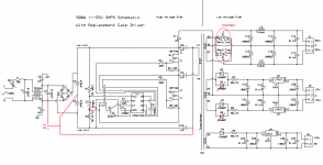
I've traced the schematic of the SMPS (second attachment) and my questions relate to the high-voltage side of the schematic, as I think I'm a bit out of my depth here.
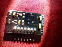
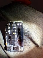
The damage included the two IRF740 MOSFETS shorted, two PCB tracks burned out, and the gate driver module destroyed. This module is a rectangular resin-encapsulated 'black box' with 7 inline pins - it has no exterior markings and I can't find any information about it.
Most of the typical SMPS designs I've seen have the junction between the mains rectified smoothing capacitors connected via a capacitor to one end of the transformer primary, and the Drain/Source junction between the two MOSFETs connected via a similar capacitor the other end of the transformer primary.
In this SMPS though, the junction between the mains rectified smoothing capacitors doesn't connect to anything else; both the +ve and -ve rails connect (via 1uF 400V capacitors) to one end of the transformer primary; and the Drain/Source junction between the two MOSFETs connected via a similar capacitor the other end of the transformer primary, same as the typical designs.
My first question is why does this SMPS have both +ve and -ve rails connected (via capacitors) to the same end of the primary transformer, and what is the effect / advantages / disadvantage of this design, versus the more typical ones?
From the schematic, I think I've figured out the pinout of the gate driver module. Pins 1&2 are joined externally on the PCB, and possibly internally in the module, and connect to R025 which I assume is a current sensing resistor. Pin 3 is V+, pin 4 V-, pin 5 is the low-side driver output, pin 6 goes to the junction of the high-side Drain and low-side Source, and pin 7 is the low-side driver output.
My second question is does anyone know a part number for this module or where I could buy a replacement? From earlier investigations, buying one from the SMPS vendor is nearly as expensive as buying a new SMPS and hardly worth the effort. But someone must be making these modules as there are many vendors of this type of SMPS on Aliexpress and eBay.
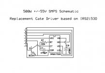
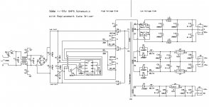
In the meantime, I've built a simple replacement based on the IRS2153D self-oscillating half-bridge driver reference model (attachment 3). I've designed the layout so that it can just plug straight into the SMPS board where the old driver was, and I've included a schematic of the SMPS with this driver (attachment 4).
My third question relates to R025 (current-sensing resistor?), which I assume is there to trigger shutdown of the IRS2153D in an over-current situation. Is my assumption correct, and will my design using BC547 work correctly? If my assumption isn't correct, what should this part of the driver schematic look like?
I've replaced both of the IRF470 MOSFETs, repaired the burnt out PCB tracks and installed my gate driver module. When I applied power, the first good thing is that there were no loud noises, and none of the magic smoke escaped. But....
The low-voltage side of the schematic has a regulated 12V output, a regulated +/-15V output and a +/-55V output which appears to be smoothed but unregulated, so the voltage presumably depends on the characteristics of the gate driver and the transformer.
... while the SMPS now seems to be working after a fashion, the +/-55V outputs quickly rise to +/-80V (or higher), at which point I quickly turn it off as I really don't understand what's happening and I'm scared it's going to blow up again!
So my fourth question is can anyone help me by explaining why the output voltage rises so much higher than it should (presumably something to do with the gate driver, as this is the only change to the original SMPS circuit), and whether there are any modifications I can make to either the gate driver or rest of the SMPS to prevent this.
Many thanks in advance,
Jon.
However, this SMPS doesn't have any effective short circuit protection, and I stupidly managed to blow up one of them by accidentally connecting it to a short circuit. That's why I've got three now - I had to buy a replacement, but I'd still like to have a go repairing this one.
I've traced the schematic of the SMPS (second attachment) and my questions relate to the high-voltage side of the schematic, as I think I'm a bit out of my depth here.
The damage included the two IRF740 MOSFETS shorted, two PCB tracks burned out, and the gate driver module destroyed. This module is a rectangular resin-encapsulated 'black box' with 7 inline pins - it has no exterior markings and I can't find any information about it.
Most of the typical SMPS designs I've seen have the junction between the mains rectified smoothing capacitors connected via a capacitor to one end of the transformer primary, and the Drain/Source junction between the two MOSFETs connected via a similar capacitor the other end of the transformer primary.
In this SMPS though, the junction between the mains rectified smoothing capacitors doesn't connect to anything else; both the +ve and -ve rails connect (via 1uF 400V capacitors) to one end of the transformer primary; and the Drain/Source junction between the two MOSFETs connected via a similar capacitor the other end of the transformer primary, same as the typical designs.
My first question is why does this SMPS have both +ve and -ve rails connected (via capacitors) to the same end of the primary transformer, and what is the effect / advantages / disadvantage of this design, versus the more typical ones?
From the schematic, I think I've figured out the pinout of the gate driver module. Pins 1&2 are joined externally on the PCB, and possibly internally in the module, and connect to R025 which I assume is a current sensing resistor. Pin 3 is V+, pin 4 V-, pin 5 is the low-side driver output, pin 6 goes to the junction of the high-side Drain and low-side Source, and pin 7 is the low-side driver output.
My second question is does anyone know a part number for this module or where I could buy a replacement? From earlier investigations, buying one from the SMPS vendor is nearly as expensive as buying a new SMPS and hardly worth the effort. But someone must be making these modules as there are many vendors of this type of SMPS on Aliexpress and eBay.
In the meantime, I've built a simple replacement based on the IRS2153D self-oscillating half-bridge driver reference model (attachment 3). I've designed the layout so that it can just plug straight into the SMPS board where the old driver was, and I've included a schematic of the SMPS with this driver (attachment 4).
My third question relates to R025 (current-sensing resistor?), which I assume is there to trigger shutdown of the IRS2153D in an over-current situation. Is my assumption correct, and will my design using BC547 work correctly? If my assumption isn't correct, what should this part of the driver schematic look like?
I've replaced both of the IRF470 MOSFETs, repaired the burnt out PCB tracks and installed my gate driver module. When I applied power, the first good thing is that there were no loud noises, and none of the magic smoke escaped. But....
The low-voltage side of the schematic has a regulated 12V output, a regulated +/-15V output and a +/-55V output which appears to be smoothed but unregulated, so the voltage presumably depends on the characteristics of the gate driver and the transformer.
... while the SMPS now seems to be working after a fashion, the +/-55V outputs quickly rise to +/-80V (or higher), at which point I quickly turn it off as I really don't understand what's happening and I'm scared it's going to blow up again!
So my fourth question is can anyone help me by explaining why the output voltage rises so much higher than it should (presumably something to do with the gate driver, as this is the only change to the original SMPS circuit), and whether there are any modifications I can make to either the gate driver or rest of the SMPS to prevent this.
Many thanks in advance,
Jon.
Attachments
I think that you have serious oscillation at the primary side causing the rise of the voltage.
Also, you can remove that BLACK epoxy using a heat gun slowly, then you can fix the module.
This circuit is pretty simple to fix, if you have an oscilloscope, you can check the waves at the IR2153 before soldering the MOSFETS.
Check all the surrounding components, you may find something else burned.
Hope that helps
I think you missed a connection, the two 1µF are to improve the HF response of C5 & C6.My first question is why does this SMPS have both +ve and -ve rails connected (via capacitors) to the same end of the primary transformer, and what is the effect / advantages / disadvantage of this design, versus the more typical ones?
Most probably.Perhaps your solution needs a low-pass to the base of the BC547 to prevent upsetting the driver by very short transient current pulses (1k + 10n ?)My third question relates to R025 (current-sensing resistor?), which I assume is there to trigger shutdown of the IRS2153D in an over-current situation.
Those circuits normally have a 115V/230V selection option.So my fourth question is can anyone help me by explaining why the output voltage rises so much higher than it should
Short for 115, open for 230V. Did you while repairing the PC also "restore" the 115V connection ?
The C7 (100µ) negative side is wrong. The 55V rectifiers are inverted and anti-parallel diodes for the 15V can't be.
Did you check the osc freq of a good supply to get it right with your replacement? 22k and 470p gives ~75kHz
Mona
Attachments
Thanks for the replies. Ketje, thanks for spotting the polarity errors in my schematic - my bad for copying and pasting some components upside down! Yes, the 115/230v link is open (230V) but there's definitely no connection from the capacitors midpoint to the transformer primary or anywhere else. So I'm still a bit puzzled by this design.
I measured the frequency of a working unit at 66KHz, and selected the Rt and Ct values based on the calculations I found on the web: f=1/(1.423*Rt*Ct) or f=1/(1.38*(Rt+75)*Ct) which make f=68-70KHz, which I thought would be close enough not to need to change any of the other components.
I've removed the MOSFETs for now, and put the scope across the driver outputs - the low-side looked pretty clean but the high-side had a very jagged waveform so there may be something else going on there. More investigation needed. Frequency measured around 68KHz as expected.
Anyway I'll have a further look when I have time next week, and would welcome any other suggestions in the meantime. And if I can't get it working I can always remove the rectifiers / capacitors and use them for a linear supply from an old Onkyo AVR transformer I've got lying around!
Thanks again.
I've got three 500W +/-55V SMPS's (first attachment) that I bought from Aliexpress and eBay, two of which have faultlessly powered my 7-channel home theater power amplifier (based on LJM's L15D IRS2092 class-D modules), for more than three years now.
However, this SMPS doesn't have any effective short circuit protection, and I stupidly managed to blow up one of them by accidentally connecting it to a short circuit. That's why I've got three now - I had to buy a replacement, but I'd still like to have a go repairing this one.
I've traced the schematic of the SMPS (second attachment) and my questions relate to the high-voltage side of the schematic, as I think I'm a bit out of my depth here.
The damage included the two IRF740 MOSFETS shorted, two PCB tracks burned out, and the gate driver module destroyed. This module is a rectangular resin-encapsulated 'black box' with 7 inline pins - it has no exterior markings and I can't find any information about it.
Most of the typical SMPS designs I've seen have the junction between the mains rectified smoothing capacitors connected via a capacitor to one end of the transformer primary, and the Drain/Source junction between the two MOSFETs connected via a similar capacitor the other end of the transformer primary.
In this SMPS though, the junction between the mains rectified smoothing capacitors doesn't connect to anything else; both the +ve and -ve rails connect (via 1uF 400V capacitors) to one end of the transformer primary; and the Drain/Source junction between the two MOSFETs connected via a similar capacitor the other end of the transformer primary, same as the typical designs.
My first question is why does this SMPS have both +ve and -ve rails connected (via capacitors) to the same end of the primary transformer, and what is the effect / advantages / disadvantage of this design, versus the more typical ones?
From the schematic, I think I've figured out the pinout of the gate driver module. Pins 1&2 are joined externally on the PCB, and possibly internally in the module, and connect to R025 which I assume is a current sensing resistor. Pin 3 is V+, pin 4 V-, pin 5 is the low-side driver output, pin 6 goes to the junction of the high-side Drain and low-side Source, and pin 7 is the low-side driver output.
My second question is does anyone know a part number for this module or where I could buy a replacement? From earlier investigations, buying one from the SMPS vendor is nearly as expensive as buying a new SMPS and hardly worth the effort. But someone must be making these modules as there are many vendors of this type of SMPS on Aliexpress and eBay.
In the meantime, I've built a simple replacement based on the IRS2153D self-oscillating half-bridge driver reference model (attachment 3). I've designed the layout so that it can just plug straight into the SMPS board where the old driver was, and I've included a schematic of the SMPS with this driver (attachment 4).
My third question relates to R025 (current-sensing resistor?), which I assume is there to trigger shutdown of the IRS2153D in an over-current situation. Is my assumption correct, and will my design using BC547 work correctly? If my assumption isn't correct, what should this part of the driver schematic look like?
I've replaced both of the IRF470 MOSFETs, repaired the burnt out PCB tracks and installed my gate driver module. When I applied power, the first good thing is that there were no loud noises, and none of the magic smoke escaped. But....
The low-voltage side of the schematic has a regulated 12V output, a regulated +/-15V output and a +/-55V output which appears to be smoothed but unregulated, so the voltage presumably depends on the characteristics of the gate driver and the transformer.
... while the SMPS now seems to be working after a fashion, the +/-55V outputs quickly rise to +/-80V (or higher), at which point I quickly turn it off as I really don't understand what's happening and I'm scared it's going to blow up again!
So my fourth question is can anyone help me by explaining why the output voltage rises so much higher than it should (presumably something to do with the gate driver, as this is the only change to the original SMPS circuit), and whether there are any modifications I can make to either the gate driver or rest of the SMPS to prevent this.
Many thanks in advance,
Jon.
What is the function of C11 here? It AC couples live mains to power supply output ground? Is that not really dangerous?
Do math.What is the function of C11 here? It AC couples live mains to power supply output ground? Is that not really dangerous?
C11 is 1nFd. What is the reactance of 1nF at 50/60Hz? On my abacus, like 2,600,000 Ohms. So even on a (rounded) 260V line, it is 100uA or 0.1mA, in a world where we avoid 5mA shocks even though dozens of mA is hardly-ever truly dangerous.
Do math.
C11 is 1nFd. What is the reactance of 1nF at 50/60Hz? On my abacus, like 2,600,000 Ohms. So even on a (rounded) 260V line, it is 100uA or 0.1mA, in a world where we avoid 5mA shocks even though dozens of mA is hardly-ever truly dangerous.
Ok regardless why do that? It results in the output gnd floating at high voltage. Resulted in a laser light show when I connected a scope (with and earthed gnd lead) to the output to try and measure noise.
it is very hard to create the proper leakage inductance for these large transformers. the 1nf cap from prim to sec shows it could be hard square wave switching, with the mains regulation as voltage regulation. otherwise it would be an LLC resonant converter operating at the frequency where the voltage is almost indepedendent of load. I have seen these also at AlieX.Can you 'scope the secondary waveforms safely for good and repaired units to compare them?
Perhaps the frequency has to be right - the transformer may be resonant with the 1uF caps.
With due respect, I think your traced schematic still has errors.
Retrace the working ones and then compare the faulty one.
You mentioned burnt tracks, you could also have some invisible (to you) hidden under components, which will confuse things.
I am a grumpy old Tech with little patience, sometimes when a repair makes me mad (which is easy") ) I plain replace instead, period.
) I plain replace instead, period.
Of course, routinely make PCBs in-house so making a new one takes 2 hours at most, from screen artwork to populated PCB.
What´s my point/suggestion?
Junk that cursed board, make a generic new one , IR2153 designs are ubiquitous, using components recycled from that one.
For me, that amounts to repair,big time.
You reuse 95% of those components, specially the complex transformer, you are just replacing the PCB, literally.
You are already convinced to make a replacement driver board ... go one step beyond, it will NOT take longer, the bonus being you will then work with a known trusted circuit
EDIT: no need to even make PCBs yourself, just get one trusted ´project and order a couple from those wonderful Chinese PCB makers, having a couple spares doesn´t hurt.
You already bought 3 complete supplies!!!!!
Retrace the working ones and then compare the faulty one.
You mentioned burnt tracks, you could also have some invisible (to you) hidden under components, which will confuse things.
I am a grumpy old Tech with little patience, sometimes when a repair makes me mad (which is easy
) I plain replace instead, period.Of course, routinely make PCBs in-house so making a new one takes 2 hours at most, from screen artwork to populated PCB.
What´s my point/suggestion?
Junk that cursed board, make a generic new one , IR2153 designs are ubiquitous, using components recycled from that one.
For me, that amounts to repair,big time.
You reuse 95% of those components, specially the complex transformer, you are just replacing the PCB, literally.
You are already convinced to make a replacement driver board ... go one step beyond, it will NOT take longer, the bonus being you will then work with a known trusted circuit
EDIT: no need to even make PCBs yourself, just get one trusted ´project and order a couple from those wonderful Chinese PCB makers, having a couple spares doesn´t hurt.
You already bought 3 complete supplies!!!!!
Hi . These power supplies are known to me , purchased two ,one as a spare , first one still operating after few years with no issues. If output voltage is too high , maybe its because of wrong frequency. These power supplies are unregulated and output voltage depends on mains voltage, operating at 50 percent duty cycle , so no inductor like in atx pc psu is needed, but no voltage regulation possible in this mode. I asked seller few years ago about this black epoxy module, in case i need spare parts ,but he said sorry ,not available, only new psu. I think too ,that ir2153 is inside. Upper mosfet driver output will have no proper waveform unless you have mosfets , so you try reduce dc voltage at input to lets say 24v , and supply black module with external 12-15v from isolated lab supply to check waveform. Too high voltage also maybe present because of some ringing and no load ,so add a small load like powerful 1k resistors.
Also to add about transformer .My version is + - 45V 500W .With noad i had about + - 46V , with heavy load - 8 ohms 100w on each rail + - 42.5V , that was much better than big toroid ,which output dropped to + - 40V with much bigger capacitors on output ... One drawback ,what these psu have ,is missing soft start , i did that by reworking pcb with two triacs integrated and 47ohm 50W resistor for startup -now i can control on off and startup with arduino in example. Also have transformer rewinded , made additional taps from power windings ,to have + - 22V ( idea to make G class from current amplifier in the future ), and seperated aux supplies gnd from power ground ,i think load on power line may introduce voltage drop on ground track and common ground transformer pin, which will reduce regulation of regulated outputs .This transformer works kinda like 50hz ones ,just winding turn ratios and mosfet and diode drop ,so if you got 80V instead of 55V , check mains voltage switch ,maybe hidden solder jumper added or bad diode bridge .
I would recommend using a 1:1 isolation transformer when building/repair/testing of offline SMPS. It allows you to use the grounded (Earth) equipment and it's a safety issue. Also a light bulb tester in series with isolation transformer helps to prevent blowouts.Ok regardless why do that? It results in the output gnd floating at high voltage. Resulted in a laser light show when I connected a scope (with and earthed gnd lead) to the output to try and measure noise.
Then THAT could be he cause of higher voltages.Also have transformer rewinded
Extra secondary or lesser primary will rise voltage, in this case 1 or 2 turns more or less have a huge impact.
We are talking primary windings with, say, 12 turns or so.
Have rewinded just power secondary winding primary untouched ,in my case turns ratio not changed , output voltages not increased, just two extra taps made ,and seperate gnd for aux. Secondary had 2x7 or 9 turns for 2x45 volts dc , can't remember right now, so primary can't have just 12 turns. What's funny ,this psu was advertised as having 100x0,1 litz wire ,but i have counted just 88 , so made my own litz wire with 100 wires.
Not me complained about rising voltages , that was op of this topic, i'm just another user of such psu ,and sharing my experience.But you are complaining about rising voltages.
Maybe that´s your problem.
maybe you missed my "primary windings with, say, 12 turns or so."
I am commenting on the scale or magnitude of windings, meaning very low turns count, not designing a bobbin for your SMPS.
As is, I was quite in the ballpark.
You just missed fact , who had problems with voltages . I have shared my experience because i have identical psu ,just different voltage version, psu pcb is looking identical.OK.
It´s often confusing when people answer at the end of "similar" but somebody else´s thread.
Much better to open a new one.
Its normal thing to answer to someone else's post ,if item is very similar , without opening new thread and possibly duplicating .
I also need to know the name of the driver they couldn't scratch off the parts inside but I don't see any numbers on the one in the middle of the others. One the end two, h24 U10 or u1D .
Center one is ustm or us1m. O think the first set of the first device is correct. I really hope someone can help us with this headache. Edit: it's U1d, us1m, and the missing transistors are 1am.
Center one is ustm or us1m. O think the first set of the first device is correct. I really hope someone can help us with this headache. Edit: it's U1d, us1m, and the missing transistors are 1am.
Attachments
Last edited:
- Home
- Amplifiers
- Power Supplies
- Help repairing a 500W +/-55V SMPS