Hi Guys,
I have a question regarding pcb trace thickness.
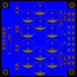
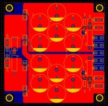
I recently designed this small psu pcb to power a pair of LM3886 boards.


100x100mm of course to take advantage of JLCpcb.
Ground plane on the bottom. +ve and -ve rails on the top.
Element 14 recently had some Panasonic AMX series 3300uF 50v caps on clearance, hence the multiple small caps instead of the usual 10000uF CDE types one might usually expect.
It will be powered by a single 25-0-25 transformer. The transformer was salvaged from an old Digitech amplifier specified as 230V @ 50 hz 300w. By weight and size I estimate the transformer is 250VA.
250VA @ 50v gives 5A AC, therefore approximately 3.25A DC at max continuous draw. I like to design for worst case conditions.
So here is my question. Will I need to use 2oz copper traces to keep temperatures low?
My thinking is that with pours nearly 50mm wide for the +ve and -ve rails, temps should stay at or close to ambient under the worst case load.
A quick run through an online calculator suggests that for a 1degree rise @ 4 amps with 1 oz copper, I would need traces 8.22mm thick.
I have a question regarding pcb trace thickness.
I recently designed this small psu pcb to power a pair of LM3886 boards.


100x100mm of course to take advantage of JLCpcb.
Ground plane on the bottom. +ve and -ve rails on the top.
Element 14 recently had some Panasonic AMX series 3300uF 50v caps on clearance, hence the multiple small caps instead of the usual 10000uF CDE types one might usually expect.
It will be powered by a single 25-0-25 transformer. The transformer was salvaged from an old Digitech amplifier specified as 230V @ 50 hz 300w. By weight and size I estimate the transformer is 250VA.
250VA @ 50v gives 5A AC, therefore approximately 3.25A DC at max continuous draw. I like to design for worst case conditions.
So here is my question. Will I need to use 2oz copper traces to keep temperatures low?
My thinking is that with pours nearly 50mm wide for the +ve and -ve rails, temps should stay at or close to ambient under the worst case load.
A quick run through an online calculator suggests that for a 1degree rise @ 4 amps with 1 oz copper, I would need traces 8.22mm thick.
It seems that most of the calculations use a 10 degree rise as a starting point.
I've noticed that most online calculators use IPC-2221 which has been superceded by IPC-2152.
A quick and dirty calculation gives a trace width of 5.3mm for 4amps with a 10 degree rise in temperature for 1oz copper using IPC-2152. For 2oz copper the trace width is 2.7mm. A 50mm trace is about 20amps for 1oz copper.
- Status
- This old topic is closed. If you want to reopen this topic, contact a moderator using the "Report Post" button.