Patrick: you're absolutely right.
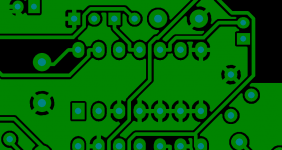
With two ground pours, one on top and the other on bottom, there's a lot of copper to suck away heat when you're soldering a pin that's electrically connected to ground. For example, check out these pins on the CD4013 IC (in a 14 pin Dual Inline Package) that are all tied to ground because there's a not-used flipflop: "U1A" on the schematic. That IC's pins certainly do have plenty heap big copper to bottom ground (green) and plenty more heap big copper to top ground (white).
Fortunately, DIY is not high volume totally automated production. When DIYers notice that solder isn't melting normally, they increase the time or the temperature or both. As you did yourself. This means we reap the benefits of mucho copper plane-of-the-ground without giant compromises for automated wave-soldering. Repeat after me: ahhhhh.
~
Attachments
What was the error? I ordered the previously posted cart.
What was the error? I ordered the previously posted cart.
C10, C11, C12 should be .1u!
Somehow in the previous iteration I had 1.5u. Perhaps Mark will say these are fine?
(This is what happens when you actually use the schematic to stuff parts! Discoveries.)
You will also find yourself with some extra 1000u caps....(Use the 25V)
Apologies.
Yea!
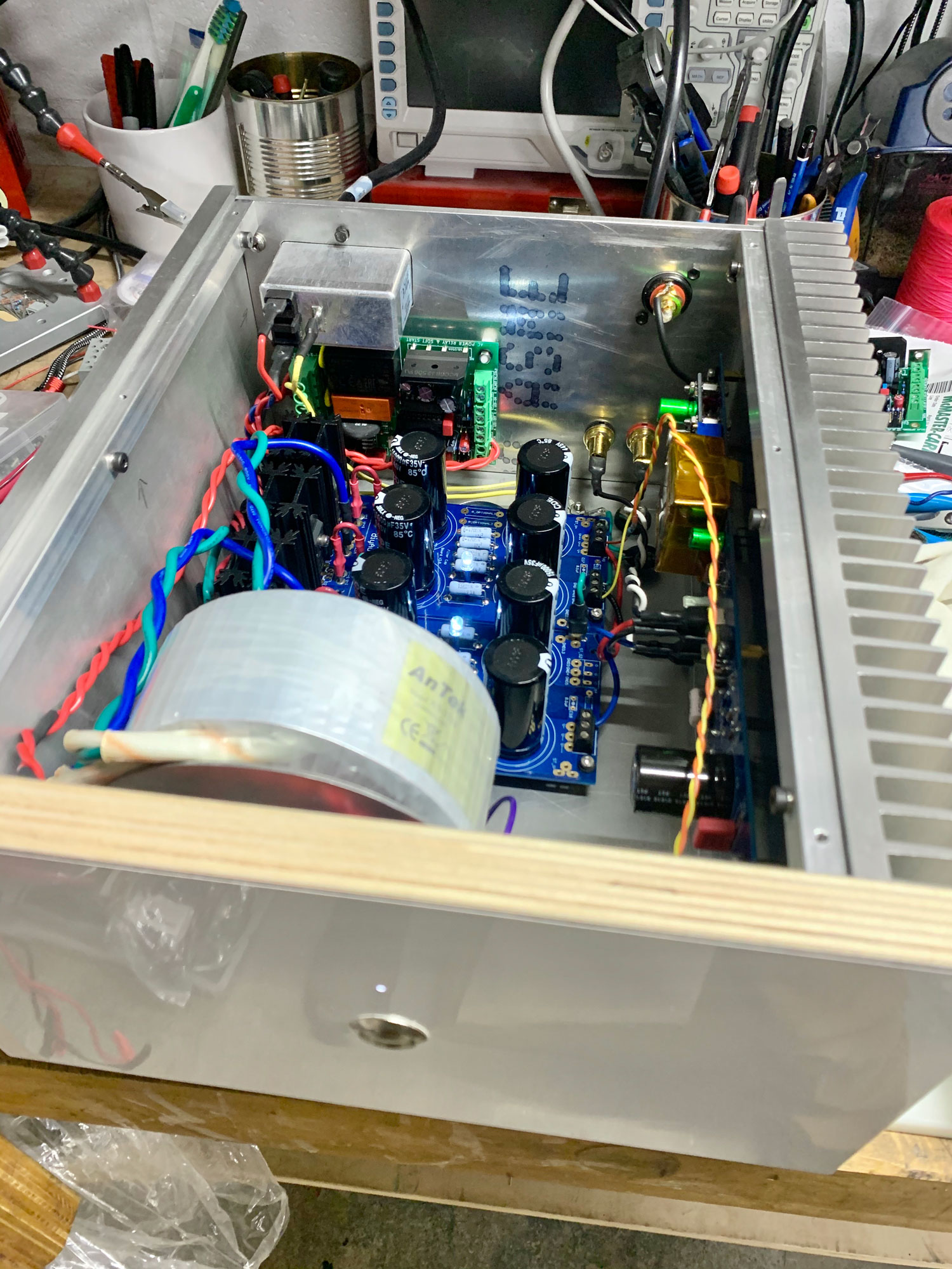
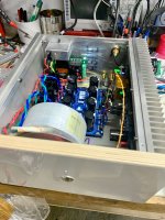
Works as expected... Have to do this again tomorrow for the other mono block.
Seems to need a couple of power on/off cycles on the front button to "time" itself for lack of a better term? Maybe it's me. I have a master switch on the IEC, now left on (Actually I left it on before too—latching switch is rated at 2A, hmmm don't think that's ideal).
Working perfectly with a satisfying little "click" as the relay trips. Pro!
(Haven't tried the LED connect yet—I like white and not bright, so I end up using around 35K, I'll add the difference in series to Mark's 4.7K)
Never had any thumps on the M2X (soft little quick hushy rush sound on power off), soft start is just a bonus in this case—AJ has an off thump... It's getting this next.
HUGE thanks Mark!! (Again.)
Attachments
C10, C11, C12 should be .1u!
Somehow in the previous iteration I had 1.5u. Perhaps Mark will say these are fine?
(This is what happens when you actually use the schematic to stuff parts! Discoveries.)
You will also find yourself with some extra 1000u caps....(Use the 25V)
Apologies.
Looking at the schematic I think these caps are in parallel after the diode rectifier for the 5v dc supply. I am not smart enough to know if the value is critical for the functionality of the soft start so I hope Mark chimes in. Aren't these there to smooth out the ripple from the rectifier a bit? Maybe if I stick a 1.5uF cap in C10 and leave C11 and C12 empty it will be fine except for the 5v line taking a bit more time to charge down?
Edit: I also have a spare .47uF 250v rated cap. Perhaps I could just use this in C10 with C11 and C12 unpopulated and be good.
Last edited:
Looking at the schematic I think these caps are in parallel after the diode rectifier for the 5v dc supply. I am not smart enough to know if the value is critical for the functionality of the soft start so I hope Mark chimes in. Aren't these there to smooth out the ripple from the rectifier a bit? Maybe if I stick a 1.5uF cap in C10 and leave C11 and C12 empty it will be fine except for the 5v line taking a bit more time to charge down?
Edit: I also have a spare .47uF 250v rated cap. Perhaps I could just use this in C10 with C11 and C12 unpopulated and be good.
They are decoupling capacitors for the digital logic.
They should not be left out and it is best to keep them 100 nF or less.
Last edited:
They are decoupling capacitors for the digital logic.
They should not be left out and it is best to keep them 100 nF or less.
Thanks. For my education where on the schematic can I see that? I see the vss and vdd points and thought those would be the takeoff points for the logic circuits and these points are before and after all 3 caps. I don't understand how the 3 100 nF caps are different than 1 300nF cap?
AJ has an off thump... It's getting this next.
Yup, the Aleph J is known for its off thump. That's not a PSU thing, but has to do how the Aleph circuit works. A slow turn on will not help with this. I added DC protection boards to my Aleph, and the hump is gone.
All amps should have DC protection for the speakers (except maybe tube amps with output transformers maybe). My F5 from the FirstWatt factory (Nelson Pass' kitchen table?) somehow decided to output DC for a while. The smell from the burnt woofer was horrible, and it was not easy to calm down SHMBO (and I must say she was right to be worried).
I like the XRK SSR DC protection boards. They are very small, are easy to work with and work very well.
Thanks. For my education where on the schematic can I see that? I see the vss and vdd points and thought those would be the takeoff points for the logic circuits and these points are before and after all 3 caps. I don't understand how the 3 100 nF caps are different than 1 300nF cap?
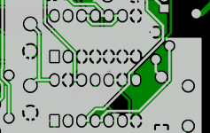
It is common practice, when drawing schematics, to put the decoupling capacitors needed, at one position on the schematic. If you look at the component placement (attached), you can see that they are physically located close to the digital ICs (U1, U3 and U5).
Attachments
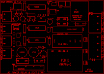
It is common practice, when drawing schematics, to put the decoupling capacitors needed, at one position on the schematic. If you look at the component placement (attached), you can see that they are physically located close to the digital ICs (U1, U3 and U5).
Ok that makes sense. Thank you.
Yes, C10 and C11 and C12 are indeed power supply bypass capacitors for the three CMOS digital logic chips. Each one is located immediately to the left of pin-14 of the chip it serves. Why pin-14? Because that's the +5V supply pin on each of these digital logic chips. The supply bypass cap is immediately adjacent to the supply pin.
In my opinion, the exact capacitance value of C10-C12 is uncritical in this circuit, and anything from 10 nanofarads (0.01 uF) up to 10 millifarads (10,000 uF) would be just fine in this circuit. There's no high-speed switching going on, there's no critical setup-time or hold-time to be violated, there's no "sag" on the +5V digital logic power supply to be counteracted, the circuit is crammed full of noise rejecting Schmitt Trigger gates, and there are straight-line, minimum length copper pathways between the pins of the bypass caps and the power&ground pins of the IC chips, in every case.
The schematic symbols for these capacitors are placed on the schematic diagram, to the right of the AC-to-DC module. That's for convenience (my convenience), and to reduce clutter on the schematic. On the board itself they are placed where they can do the most good: next to the chips they serve.
It certainly is possible to create a bad PCB layout of digital logic circuitry, such that the placement and value and routing of the bypass capacitors becomes crucial. But here we are using highly forgiving, low-speed CD4000 CMOS, switching it at a repetition rate of 0.00007 Hertz (one transition per four hours, when the on-off switch is actuated), on a PCB having a ground plane on the bottom layer and a ground pour on the top layer. Don't worry. Solder in whatever bypass capacitors you've got, and be happy.
If you're in a showy mood, select these capacitors to be a contrasting color so they really "pop" visually, next to the black epoxy ICs. 0.1uF ceramic capacitors are available in a nice bright blue color, and so are 0.1uF film capacitors. I used to really like the red AVX ceramic capacitors, 0.1uF MLCC, but can't seem to find them any more. Yellow ceramics are a little troublesome; sometimes they're bright turmeric blazing yellow, and other times they're dirty dishwater, Gulden's brown mustard yellow.
_
Last edited:
Yup, the Aleph J is known for its off thump. That's not a PSU thing, but has to do how the Aleph circuit works. A slow turn on will not help with this. I added DC protection boards to my Aleph, and the hump is gone.
All amps should have DC protection for the speakers (except maybe tube amps with output transformers maybe). My F5 from the FirstWatt factory (Nelson Pass' kitchen table?) somehow decided to output DC for a while. The smell from the burnt woofer was horrible, and it was not easy to calm down SHMBO (and I must say she was right to be worried).
I like the XRK SSR DC protection boards. They are very small, are easy to work with and work very well.
This makes sense re: AJ. I picked up a couple of XRK's boards from his Etsy shop. Thanks! Plus... Uh... Once the OSMC speaks are up and running... last thing I'd want is a smoked woofer!
... Solder in whatever bypass capacitors you've got, and be happy.
If you're in a showy mood, select these capacitors to be a contrasting color ....
_
Well that makes life easy, I will cease to worry about the exact values and think about what fashion statement I want to make
") Really appreciate the explanation, always feel better when I learn a bit (and I am starting from zero knowledge) as opposed to just plugging in the parts.
Really appreciate the explanation, always feel better when I learn a bit (and I am starting from zero knowledge) as opposed to just plugging in the parts.One more question. The amp I am building specs a CL-90 between the IEC and transformer for current inrush limiter duty. Would substituting this part for the SL22-20007 current inrush limiter be an option?
SL22-20007
https://www.mouser.com/datasheet/2/600/SL2220007-276391.pdf
CL-90
https://www.mouser.com/datasheet/2/18/AAS-920-325D-Thermometrics-NTC-Inrush-031814-web-1315885.pdf
Looking at the data sheets I see the CL-90 has a higher initial resistance of 120 ohm and a lower current rating of 2A and 36 Joules but this is within spec for the amp (Tubelab SSE) and in fact by looking at the posts on this forum has proven itself as durable in real world service. Using the 2 sec delay option will this theoretically give me an even more gentle soft start than the SL22-20007?
As long as you never harvest this board out of the Tubelab SSE chassis, and then attempt to re-use it somewhere else: sure you can use the Tubelab recommended Inrush Current Limiter part number.
However, I vigorously recommend that you create an adhesive label and stick it to the bottom side of the PCB, reminding yourself that you made a substitution. Then, four years from now, when you start amputating parts from the dead carcass of the SSE, you'll know just what has been done to this board. Without having to remember.
_
Attachments
As long as you never harvest this board out of the Tubelab SSE chassis, and then attempt to re-use it somewhere else: sure you can use the Tubelab recommended Inrush Current Limiter part number.
However, I vigorously recommend that you create an adhesive label and stick it to the bottom side of the PCB, reminding yourself that you made a substitution. Then, four years from now, when you start amputating parts from the dead carcass of the SSE, you'll know just what has been done to this board. Without having to remember.
_
Thanks, good advice. I always put together a build package for projects including the parts lists, schematics, build notes highlighting any deviations from the original design and why. For example I will include your response about the bypass capacitors and indicate the values I used in the notes for this build along with any other changes. Foresight on my part? Nope I have been bitten before.
[*]PCB mounting holes on 10 mm grid, matching Modushop perforated baseplate: Holes 60 x 90, edges 72 x 102 mm
Looks like a cool project Mark.
Is it possible to drop the PCB size on the Gerber to 72x100mm?
The reason I ask is that most PCB houses have $5 boards if you keep within 100x100mm. That extra 2mm costs an additional 19USD at the PCB house I use.
Attachments
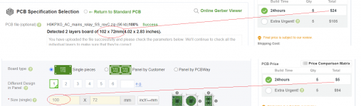
Sorry to hear it. The PCB fab that I used for my initial test run of 30 boards (JLCPCB) doesn't charge extra for (72 x 102) versus (72 x 99).
I have no plans to revise the board, unless of course a grievous bug is discovered. However please feel completely free to use this schematic and/or this parts-placement as a starting point, for developing a new PCB design and layout whose dimensions are optimized for your own needs. Wouldn't hurt my feelings at all.
I have no plans to revise the board, unless of course a grievous bug is discovered. However please feel completely free to use this schematic and/or this parts-placement as a starting point, for developing a new PCB design and layout whose dimensions are optimized for your own needs. Wouldn't hurt my feelings at all.
- Home
- Amplifiers
- Power Supplies
- PCB: low voltage On-Off switch drives AC mains relay \ includes soft start .. H9KPXG