Hey folks, we're currently in the process of designing a multi channel DAC centered around the ES9038Q2M in mono mode. The DAC will feature a motherboard with PCI express connectors, i2s-, i2c- and differential master-clock-distribution. The DAC boards themselves will be all mono channels with opto isolated i2s and i2c lines, diff-to-single-ended clock receiver, I/V and relay based volume control with 64 1dB steps. But i digress, that will be a topic for it's own thread once all the schematics and layouts are done.
Anyway, on the DAC boards we decided to use OpAmps as voltage regulators for the analog circuitry. Why you ask? Well, what comprises a good voltage regulator? It should have:
- high PSRR
- low output impedance
- high open loop gain for the feedback to work
- it should behave symmetrically on load steps, be they more or less current being demanded
- also THD seems to matter
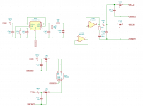
In my opinion good OpAmps should tick all of the above boxes. So, on to the actual implementation. I have attached a part of the schemtaic, the AVCC PSU. We will use the OPA1622 because of its low output impedance compared to other devices in the same family. The output stage being symmetric should help with both symmetric behaviour on load changes and it should also halve the output impedance vs. just one pass/shunt transistor.
What will have to be determined is if the ferrite bead in the AVCC output line can stay, it will probably have to be replaced by a 0 ohm resistor simply because the lowest impedance beads have a too high impedance even at audio frequencies.
What I'm wondering about is the usage of a snubber at the output of the opamp. The output of the opamp behaves as an inductance at higher frequencies which will produce overshoot and ringing in the small signal step response. So i thought the a snubber there would be beneficial. From a paper by TI i got that the snubber capacitance should roughly be three times the "parasitic" capacitance, which in this consists of 2x10u + 2x4u7, so i chose it to be 100u. The resistor value is calculated as sqrt(L/C) (it's saying 1R for the moment, please ignore the actual value for now). So the big question is how to find out the output inductance of the opamp.
I have a theory as to how to calculate that but I'm not 100% sure. Maybe somebody can shine some light on that. Also I'm looking forward to your opinion if that snubber makes any sense at all in this position.
Looking forward to your answers and stay healthy!
Anyway, on the DAC boards we decided to use OpAmps as voltage regulators for the analog circuitry. Why you ask? Well, what comprises a good voltage regulator? It should have:
- high PSRR
- low output impedance
- high open loop gain for the feedback to work
- it should behave symmetrically on load steps, be they more or less current being demanded
- also THD seems to matter
In my opinion good OpAmps should tick all of the above boxes. So, on to the actual implementation. I have attached a part of the schemtaic, the AVCC PSU. We will use the OPA1622 because of its low output impedance compared to other devices in the same family. The output stage being symmetric should help with both symmetric behaviour on load changes and it should also halve the output impedance vs. just one pass/shunt transistor.
What will have to be determined is if the ferrite bead in the AVCC output line can stay, it will probably have to be replaced by a 0 ohm resistor simply because the lowest impedance beads have a too high impedance even at audio frequencies.
What I'm wondering about is the usage of a snubber at the output of the opamp. The output of the opamp behaves as an inductance at higher frequencies which will produce overshoot and ringing in the small signal step response. So i thought the a snubber there would be beneficial. From a paper by TI i got that the snubber capacitance should roughly be three times the "parasitic" capacitance, which in this consists of 2x10u + 2x4u7, so i chose it to be 100u. The resistor value is calculated as sqrt(L/C) (it's saying 1R for the moment, please ignore the actual value for now). So the big question is how to find out the output inductance of the opamp.
I have a theory as to how to calculate that but I'm not 100% sure. Maybe somebody can shine some light on that. Also I'm looking forward to your opinion if that snubber makes any sense at all in this position.
Looking forward to your answers and stay healthy!
Attachments
Last edited:
Can't say I'm terribly convinced.
Noise wise, the LT3042 would be in the same ballpark as the OPA1622 already. If you're going to use an RC to feed the opamp, I'd rather make that 1k / 100µ, maybe even lower in impedance.
I would also consider giving "princess on a pea" type components some RC filtering of their own, or possible opt for designs with some half-decent PSRR already (so maybe not your average CMOS inverter oscillators).
Before resorting to an overdesigned contraption like this, I'd try to come up with the best possible implementation of the bare LT3042 first (C702 positioning etc.; consult datasheet).
I mean, I have nothing against this old opamp as voltage regulator trick per se (a good way of supplying fussy oscillators), but the economics of this design just don't strike me as very good. The LT3042 is almost entirely going to waste, as is the second half of the OPA1622. If you wanted high-end, you'd be using a 5 V reference and an ultra-low-Vnoise part (AD797 class). If you wanted cheap, you'd be using an 78M09/12, an R/RC divider and I dunno, an NJM4580 or a 5532 perhaps (or an OPA1688)? Something that isn't too fussed by capacitive loads in any case.
Do you have any estimate on required output current? Frying away (+18-5) V = 13 V, the thing might get a bit toasty.
Last edited:
Can't say I'm terribly convinced.
Noise wise, the LT3042 would be in the same ballpark as the OPA1622 already. If you're going to use an RC to feed the opamp, I'd rather make that 1k / 100µ, maybe even lower in impedance.
I would also consider giving "princess on a pea" type components some RC filtering of their own, or possible opt for designs with some half-decent PSRR already (so maybe not your average CMOS inverter oscillators).
Before resorting to an overdesigned contraption like this, I'd try to come up with the best possible implementation of the bare LT3042 first (C702 positioning etc.; consult datasheet).
I mean, I have nothing against this old opamp as voltage regulator trick per se (a good way of supplying fussy oscillators), but the economics of this design just don't strike me as very good. The LT3042 is almost entirely going to waste, as is the second half of the OPA1622. If you wanted high-end, you'd be using a 5 V reference and an ultra-low-Vnoise part (AD797 class). If you wanted cheap, you'd be using an 78M09/12, an R/RC divider and I dunno, an NJM4580 or a 5532 perhaps (or an OPA1688)? Something that isn't too fussed by capacitive loads in any case.
Do you have any estimate on required output current? Frying away (+18-5) V = 13 V, the thing might get a bit toasty.
OK, one by one:
I chose 10k/10u because there are decent ceramic caps available in this value, 100u might become pretty big and costly... and the opamp sees an impedance of <1k above 15.9Hz anyways, so the resistance part of the RC is not that dominant for overall impedance.
What the heck is a princess of pea device? Why are you talking about oscillators? This is the analog reference supply for the DAC. You probably got it confused with VCCA... There we will use LT3042 standalone, as for the DVCC.
The power dissipation will be below 200mW which is a piece of cacke for the OPA1622 with its thermal pad (AVCC only draws around 2mA quiescent and around 8mA output current).
How do you determince which opamp is (too) fussed about capacitive loads? How would the OPA1688 fir the bill in a better way (or the other mentioned opamps). I will stay the heck away from AD797, as it's prone to instability and I definitely don't want to risk that.
Doesn't output opamp have to be connected as integrator?
Large capacity on the opamp output and its stability. Can it work ok with such a circuistry?
Why an integrator? The Opamp is configured in gain = +1 config here, it essentially mirrors/buffers the input voltage to its output pin.
From what I read such large capacities don't pose a risk of making the opamp unstable. Phase margin is still maintained.
Why not just use the ESS datasheet opamp based psu for AVCC. I think they used an LTC6655 as 3v3 ref.
I am no expert here, just have read a lot on Mark's es9038q2m thread
The ESS datasheet does not have any schematics afaik. You probably mean the application note by ESS which uses AD797 as buffer and no extra reference, the just use DVCC and a 10k/10u RC low pass.
Why don't we plan to use the LTC6655?
a) it's not cheap and we need three references on the board
b) LT3042 is already in the bom and performs very similarly
c) with an RC low pass after the reference I doubt there will be a lot of noise difference after the RC.
From what I read such large capacities don't pose a risk of making the opamp unstable. Phase margin is still maintained.
Don't know where you read that.
http://www.ti.com/lit/ds/symlink/opa1622.pdf
High Capacitive-Load Drive Capability: > 600 pF
Does not translate to slapping 10uF on its output. If you care to sample the data sheets of a wide range of operational amplifiers you will find that most if not all recommend that when driving capacitative loads that load is isolated from the feedback node by a low value resistor, 22R or greater.
https://dl.khadas.com/Hardware/ToneBoard/Datasheet/ES-ES9038Q2M-DAC%20Datasheet.pdf
Makes little to no reference to dynamic loading of AVVC but just gives a value of 6mA. Without knowing more I would be inclined to be surprised if the DAC core is operated in a way that introduces excess spurious current draw. Rather than asking here drop an e-mail to the manufacturer.
Don't know where you read that.
http://www.ti.com/lit/ds/symlink/opa1622.pdf
High Capacitive-Load Drive Capability: > 600 pF
Does not translate to slapping 10uF on its output. If you care to sample the data sheets of a wide range of operational amplifiers you will find that most if not all recommend that when driving capacitative loads that load is isolated from the feedback node by a low value resistor, 22R or greater.
Will try to find that reference and post it here. But given that these Opamps are used frequently with such high capacitors on their output I'm not really worried about that. After all the capacitance is 4-5 orders of magnitude greater than the mentioned 600pF (which is really beasty compared to the 50pF of an 1611 for ex.)
MorbidFractal;6130037 [URL="https://dl.khadas.com/Hardware/ToneBoard/Datasheet/ES-ES9038Q2M-DAC%20Datasheet.pdf" said:https://dl.khadas.com/Hardware/ToneBoard/Datasheet/ES-ES9038Q2M-DAC%20Datasheet.pdf[/URL]
Makes little to no reference to dynamic loading of AVVC but just gives a value of 6mA. Without knowing more I would be inclined to be surprised if the DAC core is operated in a way that introduces excess spurious current draw. Rather than asking here drop an e-mail to the manufacturer.
Well. the current can swing from 0 to 7.8mA if operating into a virtual ground in mono mode. See datasheet page 52, to the end of the page.
I didn't find the original reference, but here's one that might help:
Simulation Shows How Real Op Amps Can Dri - Maxim Integrated
Note the plots to the end of the document. Given that the capacitance is >50uF here and that the opamp has an internal open loop output impedance in the order of at least several ohms the pole that is formed by this RC network is so low in frequency that the circuit cannot oscillate. At least that's how I understood it.
The 1622 also has a higher output drive current than the 1611, x5, and what looks like 1/5 the GBW. If you can find the reference then... but 4-5 orders of magnitude, 1E4 - 1E5, has to be a pipe-dream. Perhaps you are refering to an application where the device drives a 10-100uF DC blocking capacitor but the circuit includes series resistance in the coupled stage.
In terms of output current into a virtual ground I think the virtual ground is referenced to AVVC/2 so +/-3.86mA. However what is drawn from the supply does not necessarily follow what is delivered to the output.
...Sorry missed your last post. I'll have a look.
In terms of output current into a virtual ground I think the virtual ground is referenced to AVVC/2 so +/-3.86mA. However what is drawn from the supply does not necessarily follow what is delivered to the output.
...Sorry missed your last post. I'll have a look.
Last edited:
As you can see from the reference you give the opamp still needs the isolating resistor if feedback is taken from the output of the opamp. Don't confuse Rout with the additional resistor, R3. The additional feedback only helps at low frequencies. Again don't confuse Rout with R3 but yes the additional feedback works because its contribution to loop gain rolls off before the loop hits zero.
OK, I have to admit that my math knowledge is hardly any better than what I got from college (gymnasium in Germany). So could you please explain, why the circuit in the ESS app note (http://www.esstech.com/files/4514/4095/4306/Application_Note_Component_Selection_and_PCB_Layout.pdf - page 4) does work in the real world with no additional resistor? Also other opamps like the OPA1611 or the LME49720 seem to cope well with this config.
I'm eager to fully understand this topic!
I'm eager to fully understand this topic!
Ouch! Some opamps don't like it but if you slug them hard enough they submit. Shades of let's just throw dominant pole compensation out of the window by introducing a bigger dominant pole. You may even find that slew rate limiting of the output stage comes into play.
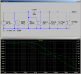
Opamps of the non esoteric kind generally use something called dominant pole compensation. It's something applied to the input stage such that irrespective of what the rest of the circuit does the AC response is dominated by that pole for all frequencies up to the zero gain crossover. Everything is nice and first order with a 90 degree phase shift up until that point. Something like the first picture. Above about 1MHz other things come into play, including pole splitting, but otherwise Cdom dominates the response.
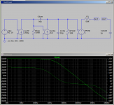
As you have noted the intrinsic output impedance, not the added resistor, of the opamp forms an additional pole at some frequency with a load capacitor and it is possible for that to render the loop second order. Your Maxim note gives a hint of this where they add an emitter follower and bias it into Class A. That's tied in with the intrinsic emitter resistance which is set by collector current. Second picture shows the result. This time the loop goes second order and crosses zero gain with 0 degrees. When you apply feedback to that it will be unstable.
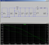
Third picture shows what these animals are trying to do. You just whack up the value of the load capacitance to a level where it, in conjunction with the intrinsic emitter/output resistance, becomes the new dominant pole and you gain back some phase margin and stability. In this case I've dumped 1000uF on my model to do it and, of course, depending on the characteristics of the actual device you use things will be subject to variation.
Faced with something like this I would be inclined to revisit the original problem and ask some questions about what solution was being sought before this answer was chosen because at face value the fourth picture is just idiot speak for I don't know stuff but if I put a big enough capacitor on this most expensive part of the circuit I cripple it but that works.
When I first posted on this forum I went a bit ape at people building semi-discrete regulators suing opamps with no local feedback and paying no overall attention to the overall loop gain. This is a similar situation. Consider your 1162. It's got a Gain Bandwidth Product of 80 Freaking MEGA HERTZ and the first thing you do is throw that in the bin.
Opamps of the non esoteric kind generally use something called dominant pole compensation. It's something applied to the input stage such that irrespective of what the rest of the circuit does the AC response is dominated by that pole for all frequencies up to the zero gain crossover. Everything is nice and first order with a 90 degree phase shift up until that point. Something like the first picture. Above about 1MHz other things come into play, including pole splitting, but otherwise Cdom dominates the response.
As you have noted the intrinsic output impedance, not the added resistor, of the opamp forms an additional pole at some frequency with a load capacitor and it is possible for that to render the loop second order. Your Maxim note gives a hint of this where they add an emitter follower and bias it into Class A. That's tied in with the intrinsic emitter resistance which is set by collector current. Second picture shows the result. This time the loop goes second order and crosses zero gain with 0 degrees. When you apply feedback to that it will be unstable.
Third picture shows what these animals are trying to do. You just whack up the value of the load capacitance to a level where it, in conjunction with the intrinsic emitter/output resistance, becomes the new dominant pole and you gain back some phase margin and stability. In this case I've dumped 1000uF on my model to do it and, of course, depending on the characteristics of the actual device you use things will be subject to variation.
Faced with something like this I would be inclined to revisit the original problem and ask some questions about what solution was being sought before this answer was chosen because at face value the fourth picture is just idiot speak for I don't know stuff but if I put a big enough capacitor on this most expensive part of the circuit I cripple it but that works.
When I first posted on this forum I went a bit ape at people building semi-discrete regulators suing opamps with no local feedback and paying no overall attention to the overall loop gain. This is a similar situation. Consider your 1162. It's got a Gain Bandwidth Product of 80 Freaking MEGA HERTZ and the first thing you do is throw that in the bin.
Attachments
Thanks very much for simulating that! Things just got a tad clearer for me...
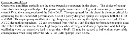
I'll take a step back though and explain why we arrived at the values for the caps that were chosen as of now. So what is it that we are seeking for? Well, the ideal voltage source which has zero output impedance over the needed frequency range. As zero is not possible, let's look at a more realistic approach.
The ESS has 0dB PSRR on the AVCC pin, it's a reference voltage. So to achieve a SNR of 125dB for example the noise voltage on the AVCC pin must not exceed 3.3V/125dB which equals 1.8uV. if we say the current swing demanded by the AVCC pin is 8mA the output impedance of the regulator must no exceed 0.2mOhms or otherwise the current will modulate the voltage by more than these 1.8uV (Hope there is no error in my calculation). Even if I would use an Opamp with no capacitance at all it will not be able to have such a low Zout over the whole frequency range that we need it to operate at. Keep in mind that this is a SD DAC which modulates in the MHz region. So we quickly came to the conclusion that there's no way we would get away without a cap across the AVCC supply. So we did quite a long search to find a suitable capacitor combination that a) does not induce resonances from the package inductances and will b) have a low impedance over a wide frequency range. That's why we ended up with a 1812 10uF MLCC in parallel with a four terminal feedthrough cap from TDK, 0603 package, 4.7uF.
So what are our options now? as far as I can see it's either no cap at all, let the opamp (or regulator for that matter) do it's thing, accept it's rising Zout at higher frequencies or try to make it stable with some carefully chosen capacitor values.
I'll throw one more question in, just for the fun of it:
If I add a ferrite bead in series with the output of the opamp, that would likely make it stable too, right? because the ferrite bead will show resistive behaviour from a few hundred kHz on. Of course ideally the resistance would only rise above a frequency where the caps already show very low impedance. In reality I didn't find a bead that shows really low impedance up into the MHz range. :/
Last edited:
- Status
- This old topic is closed. If you want to reopen this topic, contact a moderator using the "Report Post" button.
- Home
- Amplifiers
- Power Supplies
- Using OpAmps as Voltage Regulators