My problem was that I didn't know how to enter the expressions to plot.
The expression is correct but you don't plot what you seem to want to plot. If you plot the two terminals of a voltage source, you just see the voltage source. You need to select the nodes you want to plot.
Jan
FWIIW If you assume that the PDM stream consists of what can be approximated to a 0-VREF level switched to the input of a 774R resistor, RDAC, then fed into a current to voltage convertor then the attached model might make you cry... It assumes a 50% duty cycle PDM at 1MHz and the large signal behaviour is not pretty.
Attachments
OK, tried to run the file you just provided. The simulation runs, however I get a warning: Less than two connections to node BFO. But I guess you use that to show the voltage difference between 3.3V and V(BUF)?
Anyway, I get no traces to show up at all, regardless of what I add to it... Not even a flat line. What am I doing wrong?
Anyway, I get no traces to show up at all, regardless of what I add to it... Not even a flat line. What am I doing wrong?
Yes. It is to show the difference. Also sometimes LTSpice messes up the scaling when you are trying to see low level detail on a large offset. When you run it does the waveform viewer come up after some time and is it empty, no plots. It is possible that because you just have the .asc file and the .raw file has not yet been generated it does not know what to plot yet. Once the analysis has completed you should be able to click on nodes an display traces. It also will not start displaying waveforms until it has reached Tstart, 100uS. If you have a slow computer then it might take a while to reach that point. You might try increasing the maximum timestep in the .tran statement.
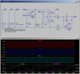
OK, small update - we can see the PDM voltage, but no other trace. What's weird is, that it doesn't show a flat line, just no line at all. Also how did you achieve to split these traces out onto multiple planes? Attached is what we can see here...
Btw. my computer does ~1.1us/s - is that slow or fast?")
Btw. my computer does ~1.1us/s - is that slow or fast?
Attachments
Mine does 7.5uS/S but it uses 4 cores on a fast processor. It is strange that it says it is plotting the waveforms and then does not plot them. To get multiple planes right click on the background and just below add traces you will see add plot plane. You can drag traces from one plane to another.
OK, this is on a laptop processor and only 4 cores of it are assigned to the vm.
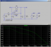
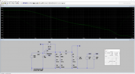
But back to the earlier simulation, the basicloop. As one can see in the gain/phase plot with the 100u cap you provided, the gain starts to rise again after some frequency. is that to be expected? What does this mean? And yet another thing, which _might_ explain the weird behaviour - should the cap not be connected between the output of the opamp and GND? In the .asc file you provided it's essentially connected between the negative input and ground, separated by the voltage source.
But back to the earlier simulation, the basicloop. As one can see in the gain/phase plot with the 100u cap you provided, the gain starts to rise again after some frequency. is that to be expected? What does this mean? And yet another thing, which _might_ explain the weird behaviour - should the cap not be connected between the output of the opamp and GND? In the .asc file you provided it's essentially connected between the negative input and ground, separated by the voltage source.
OK guys. We did a lot of playing around with different component values and think we learned quite a bit from that.
The idea of using OpApms as voltage regulator still seems to be quite viable though and I have not given up on it (yet?).
A few basic questions arose from all the fiddling around, reading and trying to understand stuff.
1. What's the fundamental difference between
a) an opamp in positive gain configuration (gain +1 in our mentioned case) amplifying a voltage reference on its + input
and
b) a "regular" voltage regulator?
The voltage reg also has a reference, an error amplifier and an output stage. I'd guess that the error amplifier also has a pole (which means that it's bandwith is limited?!). Doesn't the output capacitor add another pole there? Can't seem to wrap my head around the fundamental difference there.
2. We compared the achievable output impedance of "our" circuit (which is in no way to say I invented it) to some of the highly regarded discrete voltage regs out there. I could never find any graphs above 100k, so it seems to they are purely designed for analog circuits and audio frequency demands. Does anybody have simulated or measured Zout(f) plots above 100kHz? Are these regulators also susceptible to the capacitance on their output, if so - how?
3. There seems to be at least some discrepancy between the theory/simulation and real world performance. AD797, OPA1611, LME49720 all seem to work with significantly higher capacitance on their outputs than the simulation suggests. Who's wrong and why? How much phase margin is actually needed to pervent an opamp from oscillating? From what I understand the step response becomes worse and worse with a lot of ringing if I approach 180° phase, is that correct?
4. To the sim experts, why is the voltage source for simulating open loop gain connected in such a weird way, inside the feedback loop? Naively I would have connected it between +/- inputs.
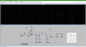
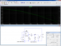
5. My buddy did a lot of the tiring task of simulating different versions of the schematic, he deserves all the credit for patience there. Attached is a probably working example of it, in which we tried to use real world capacitor values and some inductance for the lead from the reg to the load. I'd really like your comments on that. Is a phase margin of 8° considered enough?
Hope you all bear with me here, it's an exciting ride and I'm certainly learning a lot here...
The idea of using OpApms as voltage regulator still seems to be quite viable though and I have not given up on it (yet?).
A few basic questions arose from all the fiddling around, reading and trying to understand stuff.
1. What's the fundamental difference between
a) an opamp in positive gain configuration (gain +1 in our mentioned case) amplifying a voltage reference on its + input
and
b) a "regular" voltage regulator?
The voltage reg also has a reference, an error amplifier and an output stage. I'd guess that the error amplifier also has a pole (which means that it's bandwith is limited?!). Doesn't the output capacitor add another pole there? Can't seem to wrap my head around the fundamental difference there.
2. We compared the achievable output impedance of "our" circuit (which is in no way to say I invented it
) to some of the highly regarded discrete voltage regs out there. I could never find any graphs above 100k, so it seems to they are purely designed for analog circuits and audio frequency demands. Does anybody have simulated or measured Zout(f) plots above 100kHz? Are these regulators also susceptible to the capacitance on their output, if so - how?3. There seems to be at least some discrepancy between the theory/simulation and real world performance. AD797, OPA1611, LME49720 all seem to work with significantly higher capacitance on their outputs than the simulation suggests. Who's wrong and why? How much phase margin is actually needed to pervent an opamp from oscillating? From what I understand the step response becomes worse and worse with a lot of ringing if I approach 180° phase, is that correct?
4. To the sim experts, why is the voltage source for simulating open loop gain connected in such a weird way, inside the feedback loop? Naively I would have connected it between +/- inputs.
5. My buddy did a lot of the tiring task of simulating different versions of the schematic, he deserves all the credit for patience there. Attached is a probably working example of it, in which we tried to use real world capacitor values and some inductance for the lead from the reg to the load. I'd really like your comments on that. Is a phase margin of 8° considered enough?
Hope you all bear with me here, it's an exciting ride and I'm certainly learning a lot here...
Attachments
None: a VR is just a (very) peculiar type of 1-quadrant opamp1. What's the fundamental difference between
a) an opamp in positive gain configuration (gain +1 in our mentioned case) amplifying a voltage reference on its + input
and
b) a "regular" voltage regulator?
Yes, but the regulator has been designed with the knowledge that it would have to drive ~unlimited amounts of capacitance, and this heavily influences the tradeoffs.The voltage reg also has a reference, an error amplifier and an output stage. I'd guess that the error amplifier also has a pole (which means that it's bandwith is limited?!). Doesn't the output capacitor add another pole there? Can't seem to wrap my head around the fundamental difference there.
Many regulators have requirements on the output cap, precisely because it introduces an additional pole.
Above a certain frequency, it becomes more advantageous to use passive bypassing means, knowing that some bypassing will be needed anyway for VHF+, and the regulator will need to be able to cope with that capacitance.2. We compared the achievable output impedance of "our" circuit (which is in no way to say I invented it
Reality is the ultimate acid test, but if the phase margin is too low, stability is not sufficient and sim is a good indicator of what to expect.3. There seems to be at least some discrepancy between the theory/simulation and real world performance. AD797, OPA1611, LME49720 all seem to work with significantly higher capacitance on their outputs than the simulation suggests. Who's wrong and why? How much phase margin is actually needed to pervent an opamp from oscillating? From what I understand the step response becomes worse and worse with a lot of ringing if I approach 180° phase, is that correct?
Depending on how you see things and how the phase-wrapping of the simulator works, the stability is zero when the phaseshift around the loop reaches 180°, or when the phase difference between the input and output is 0°
Yes, but you need to keep the amplifier in its linear zone, something not so obvious if it has a gain of 10,000,0004. To the sim experts, why is the voltage source for simulating open loop gain connected in such a weird way, inside the feedback loop? Naively I would have connected it between +/- inputs.
8° would not be enough, but your sims are incorrect: for the impedance you cannot mix a current stimulus and a voltage on a different node (otherwise you measure transimpedance instead of impedance), and for the loop gain you need to break the loop at the point of feedback (split that node), not on different, existing nodes5. My buddy did a lot of the tiring task of simulating different versions of the schematic, he deserves all the credit for patience there. Attached is a probably working example of it, in which we tried to use real world capacitor values and some inductance for the lead from the reg to the load. I'd really like your comments on that. Is a phase margin of 8° considered enough?
Want to address two of your statements:
1. if 8° is not enough - how much is enough?
2. If the simulation shows that the circuit does not work, how do people obviously still get away with that? What real world differences might make it work, or in other words - where does the simulation model fall short?
3. regarding the last statement: We turned off the voltage source and enabled the current source for Zout simulation and vice versa (Can be seen from the 0 or 1 value next to it in the screenshots). So I think this is in fact correct. Please correct me if I'm wrong.
#51
1) As you suggest the lack of difference is that each is subject to considerations about what comprises the feedback loop and how those components affect the overall loop gain and phase.
2) Is kind of 1). You will generally find that recommendations are made as to minimum/maximum values of capacitance and associated ESR can be placed on the output of such regulators.
Whilst they may not give data above 100KHz it is likely that they could perform just as well as your circuits. Check the transient model and measure how much current your op-amp is supplying vs how much is being supplied by the capacitors. Hover should give you a current clamp meter.
3) Could be part of #53...
4) I am a Monkey. I think I have already proved that one having got it wrong before. As such I kind of follow orders...
LTspice: Extracting Switch Mode Power Supply Loop Gain in Simulation and Why You Usually Don't Need To | Analog Devices
I guess, without hunting down the original, the important bit is...
5) Is #53
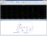
#53
1) Rumour has it that for critical damping you want to cross over first order with 45 degrees phase margin. That one assumes the loop is, can be, second order at half of and twice that frequency.
2) Your 8 degree figure results from the cursor being in the wrong place. You appear to have measured the minimum phase. What you should look at is what the phase is when the gain crosses 0dB. On the second picture that is where the phase has bumped back up to 60 degrees.
3) Yes. Depending on what you are measuring you set the appropriate disturbing source to get the answer and the other source(s) to zero.
1) As you suggest the lack of difference is that each is subject to considerations about what comprises the feedback loop and how those components affect the overall loop gain and phase.
2) Is kind of 1). You will generally find that recommendations are made as to minimum/maximum values of capacitance and associated ESR can be placed on the output of such regulators.
Whilst they may not give data above 100KHz it is likely that they could perform just as well as your circuits. Check the transient model and measure how much current your op-amp is supplying vs how much is being supplied by the capacitors. Hover should give you a current clamp meter.
3) Could be part of #53...
4) I am a Monkey. I think I have already proved that one having got it wrong before. As such I kind of follow orders...
LTspice: Extracting Switch Mode Power Supply Loop Gain in Simulation and Why You Usually Don't Need To | Analog Devices
I guess, without hunting down the original, the important bit is...
I think that if you look back to your Maxim reference they implement the method according to Middlebrook.Determining the open loop response of a linear, closed loop system is a problem solved well by Middlebrook's method[2]. That method uses test signals injected into the closed loop system to independently solve for the voltage and current gains. These two gains are then convoluted together to get the true loop gain. If a point in the feedback loop can be identified where a low impedance drives a high impedance, then the current gain is zero and it is sufficient to measure only the voltage gain and identify that as the loop gain. Such a point can normally be found in a SMPS since you have a power supply output driving an error amplifier input.
5) Is #53
#53
1) Rumour has it that for critical damping you want to cross over first order with 45 degrees phase margin. That one assumes the loop is, can be, second order at half of and twice that frequency.
2) Your 8 degree figure results from the cursor being in the wrong place. You appear to have measured the minimum phase. What you should look at is what the phase is when the gain crosses 0dB. On the second picture that is where the phase has bumped back up to 60 degrees.
3) Yes. Depending on what you are measuring you set the appropriate disturbing source to get the answer and the other source(s) to zero.
It depends on your personal comfort zone: in general, 60° is deemed OK, but higher values, closer to 90° are preferable.Want to address two of your statements:
1. if 8° is not enough - how much is enough?
45° is still workable, and 30° is the absolute limit beyond which you shouldn't venture, because of dispersion, etc.
The sim might indicate 8° as in your case (except that your sim was wrong and the frequency was incorrect), and in the real world, the circuit won't oscillate: it will just show a horrendous behavior in the vicinity of the 0dB crossing region.2. If the simulation shows that the circuit does not work, how do people obviously still get away with that? What real world differences might make it work, or in other words - where does the simulation model fall short?
Real world circuits sometimes have additional hidden damping that help save the day, and models aren't 100% complete or accurate anyway
I'll give examples of the proper (simplified) way of measuring loop gain and out Z.3. regarding the last statement: We turned off the voltage source and enabled the current source for Zout simulation and vice versa (Can be seen from the 0 or 1 value next to it in the screenshots). So I think this is in fact correct. Please correct me if I'm wrong.
I use a simplified setup and a native LT device for simplicity, but you can apply the same principles to more complex situations.
This the loop gain:
And this is the output impedance:
Attachments
- Status
- This old topic is closed. If you want to reopen this topic, contact a moderator using the "Report Post" button.
- Home
- Amplifiers
- Power Supplies
- Using OpAmps as Voltage Regulators