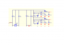
R1 together with the capacitors C1 C3 filter out ripple. Q1 acts as an emitter follower to boost the current (capacitance multiplier).
Under heavy load (and during start up) R3 and D2 conduct and allow more current to flow (and faster startup). Under high load the ripple filtering is ineffective due to the short time constant of R3 x C1
D1 protects Q1 from reverse bias at shutdown.
C2 stiffens up the rail at high frequencies.
Under heavy load (and during start up) R3 and D2 conduct and allow more current to flow (and faster startup). Under high load the ripple filtering is ineffective due to the short time constant of R3 x C1
D1 protects Q1 from reverse bias at shutdown.
C2 stiffens up the rail at high frequencies.
The specific power supply is the supply that feeds the primary side of one amplifier so " Heavy load" is something very relative here
Most important for me to understand is how this power supply stabilizes voltage from 58 volt rails to 45 volt output
schematic is drawn correctly factory made operating amplifier
how R3 and D2 will sense heavy load if not connected to it ? If any load that appears only at the emitter of the transistor . Any drive at base has no sense of what is going on in the output Something doesn't make sense here .
Good analysis by Mark.
When R1 carries 0.1 mA for the base of Q1, it has a voltage close to the 3.6 Volt threshold of D2. 0.1mA in the base of R1 means an output current in the order of 10-30mA. At that moment R2 starts supplying current (through D2) to the base of Q1 as well. This extra current avoids that the output voltage collapses but with the result that the ripple filter has little effect.
In Marks explanation, I believe “..R3 and D2 conduct.." should be “..R2 and D2 conduct..” and “R3xC1” should be “R2xC1”.
My impression is that the left sides of R1 and R3 should eventually be connected to ground instead of the supply voltage.
When R1 carries 0.1 mA for the base of Q1, it has a voltage close to the 3.6 Volt threshold of D2. 0.1mA in the base of R1 means an output current in the order of 10-30mA. At that moment R2 starts supplying current (through D2) to the base of Q1 as well. This extra current avoids that the output voltage collapses but with the result that the ripple filter has little effect.
In Marks explanation, I believe “..R3 and D2 conduct.." should be “..R2 and D2 conduct..” and “R3xC1” should be “R2xC1”.
I question if the schematic is drawn correctly... It would make much more sense if R2 and R4 were connected to ground.
My impression is that the left sides of R1 and R3 should eventually be connected to ground instead of the supply voltage.
The transistor base current rises, increasing the voltage drop across R1 until the zener voltage is reached and R3 can start to conducthow R3 and D2 will sense heavy load if not connected to it ?
Base certainly knows about the load. Base current is directly related to the load current in the linear region.If any load that appears only at the emitter of the transistor .
Any drive at base has no sense of what is going on in the output
Something doesn't make sense here .
- Status
- This old topic is closed. If you want to reopen this topic, contact a moderator using the "Report Post" button.
- Home
- Amplifiers
- Power Supplies
- PSU principal of operation