Do you mean IN ADDITION to Sadface's existing 10Ω series resistor between the 2200uF caps?If you add a series resistor before the input cap, like 1R, the improvement would be much better than increasing the input capacitor.
I was already going to lower that 10Ω resistor to 1Ω, because with a 1 amp draw, I can't afford the 10 volt drop.
Diego had proposed that simpler arrangement: an RC instead of a CRC one. As I had been one of those that had simulated CRC filters before Diego's suggestion, I had to think it over.
In spite of being more effective, cutting the high frequency ripple quite a lot, as Elvee had mentioned: anything below -100dB is more than enough. Going much lower won't make much of a difference audio wise, and you will reducing your assembly space when you are designing a new supply pcb, and also spending less in parts. In this case just one cap, smaller.
It sounds like a good bargain.
For most traditional supplies, the all-important PSRR figure is the 100Hz (or 120Hz) one.
If in addition you can get stellar 10kHz figures for free, why not, but as soon as you have to increase the losses to get there it becomes unattractive.
If the 100dB of the denoiser isn't enough, the realistic solution is to use an even better regulator: either a "traditional" superreg in the Jung style, or a Dienoiser/nonoiser.
If the primary source is a SMPS operating at tens or hundreds kHz, a good LC filter will greatly increase rejection with a moderate L value.
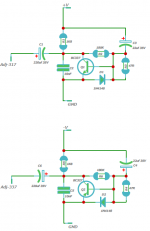
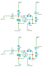
Sadface, I am wondering if you could turn your obviously superb layout skills to making gerber files for a couple of small retro-fit PCBs using Elvee's brilliant and simple de-noiser circuitry. One for the LM317 side, and one for the LM337 side. I was thinking that splitting the two might make it easier to fit various existing voltage regulator boards; maybe it would be too costly; I don't know. All eight components on each board, including the C3 220µF coupling capacitor to the adjust regulator pin. That way, the board could just replace the existing capacitor (with the additional connection to the regulator output), or be wired in parallel with the voltage-setting resistor R2 if there is no cap on the existing board.I have made a dual rail pcb that works as intended.
Attached are the gerber files that can be used to order pcbs from a PCB fab
Whattya think? I'd do it myself, but I don't know how!
My denoiser boards using your gerber layouts are on order; probably take a few weeks to arrive, though. Perfect for use in my new builds, or to replace very old regulator boards; but I have numerous existing LM317/337 regulator boards that could well benefit from the denoiser.
Last edited:
Exactly: that was the initial intention, a retrofittable module.
Sadface, you would do a great service to the community by designing such an add-on PCB.
You could even sell them at a honest price: I see absolutely no inconvenient to it (and I am not going to ask any percentage on your sales!)
Sadface, you would do a great service to the community by designing such an add-on PCB.
You could even sell them at a honest price: I see absolutely no inconvenient to it (and I am not going to ask any percentage on your sales!)
@Hiroco
You have shorted R3 and R4. The base of the transistors should not be connected to R2, R3 and C3 (or R4, R6 and C4 for the 337 version).
A great circuit idea by Elvee by the way.
I have simulated the Dienoiser in Tina TI. I tried with different transistors, including BC337-40 and FZT851. The latter gave very good results as others have reported earlier.
For fun I tried to use the 2SD2704 (a mute transistor with very high gain). In my simulation it performed very well, with a lower noise than the FZT851.
Interesting find: this transistor combines a very high Hfe with the high Vebo required for muting applications, two properties that are usually mutually exclusive.For fun I tried to use the 2SD2704 (a mute transistor with very high gain). In my simulation it performed very well, with a lower noise than the FZT851.
If in addition it also has an exceptionally low Rbb, it is a truly miraculous device!
Thanks @Jenst and @Carlmart...for your expertise.
Is that correct now?
The diodes should be directly across the base emitter of the transistors. In normal operation they have no influence on the circuit behavior. They are there to protect the transistors against (transient) reverse voltage on the BE.
Sure, I just need the approval from Elvee to post the PDF and the Gerbers FilesEXCELLENT! Gerber files?
Sadface, I am wondering if you could turn your obviously superb layout skills to making gerber files for a couple of small retro-fit PCBs using Elvee's brilliant and simple de-noiser circuitry. One for the LM317 side, and one for the LM337 side. I was thinking that splitting the two might make it easier to fit various existing voltage regulator boards; maybe it would be too costly; I don't know. All eight components on each board, including the C3 220µF coupling capacitor to the adjust regulator pin. That way, the board could just replace the existing capacitor (with the additional connection to the regulator output), or be wired in parallel with the voltage-setting resistor R2 if there is no cap on the existing board.
Whattya think? I'd do it myself, but I don't know how!
My denoiser boards using your gerber layouts are on order; probably take a few weeks to arrive, though. Perfect for use in my new builds, or to replace very old regulator boards; but I have numerous existing LM317/337 regulator boards that could well benefit from the denoiser.
You flatter me, I am merely an inexperienced amateur with probably just enough knowledge to be truly dangerous.
I'd be happy to design a denoiser addon board however this raises questions as to how one would want it implemented in terms of connections, mounting and size etc
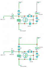
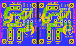
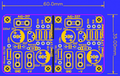
I see that Hicoco has stepped up in my absence and designed a splitable board for separate rails.
Does anybody want or require a dual rail addon board with a single centre ground rail or are we happy with Hicoco's fine looking offering?
Other questions I could ask would be do we want boards designed for minimum size and therefore less options for component choice or would we prefer boards that are larger but able to accommodate varied footprints?
How would the addon boards be best mounted? Vertically mounted using jumpers to connect to the parent board or horizontally mounted on screws and spacers and then wired to the parent board using screw terminals or faston spade connectors?
I've been having issues recently with EasyEDA running exceptionally slow. I suspect this might be a function of how I use the software. I have a habit of copying and pasting sections of wire both large and small as fill, especially around smaller traces etc. My suspicion is that his creates too many objects and bogs the system down.
I've downloaded Kicad but that is a different kettle of fish. It seems to have a much steeper learning curve. More importantly whilst I can copy over my pcb layout from EasyEDA. I have not yet been able to export my schematics and from my experimentation so far, Kicad doesnt recognise the nets from EasyEDA.
I am going to have to persevere with EasyEDA for the current board I am designing (a clone of the AMB labs Sigma 22 board designed to accommodate 35mm capacitors) and then I will bend my mind to learning Kicad.
Last edited:
I've downloaded Kicad but that is a different kettle of fish. It seems to have a much steeper learning curve. More importantly whilst I can copy over my pcb layout from EasyEDA. I have not yet been able to export my schematics and from my experimentation so far, Kicad doesnt recognise the nets from EasyEDA.
I am going to have to persevere with EasyEDA for the current board I am designing (a clone of the AMB labs Sigma 22 board designed to accommodate 35mm capacitors) and then I will bend my mind to learning Kicad.
I've not looked hard enough myself but could LibrePCB have a less steep learning curve?
LibrePCB
For the moment it appears to be less advanced but that might work in its favour.
You don't need my approval since it is a completely open project, but I give it anywaySure, I just need the approval from Elvee to post the PDF and the Gerbers Files
Mounting: screws are possible but overkill, double-sided adhesive tape, electronic putty, silicone, thermal glue etc. are probably easier and sufficient.mounting and size etc
Size: a small as practical to be used even in cramped spaces
Splittable is excellent: it leaves all your options openI see that Hicoco has stepped up in my absence and designed a splitable board for separate rails.
A common ground could simplify the wiring in some situations, but it comes with restrictions and possible issues like non-optimal ground connection.Does anybody want or require a dual rail addon board with a single centre ground rail or are we happy with Hicoco's fine looking offering?
Keep separate grounds
A difficult one: some builders don't care about VLF response or peaking, others do.Other questions I could ask would be do we want boards designed for minimum size and therefore less options for component choice or would we prefer boards that are larger but able to accommodate varied footprints?
The boards should be as small as possible, yet tolerate the 220µF (the largest cap), and perhaps 330µ or 470µ (optional)
Many mounting methods should be possible, to accomodate a maximum of real situationsHow would the addon boards be best mounted? Vertically mounted using jumpers to connect to the parent board or horizontally mounted on screws and spacers and then wired to the parent board using screw terminals or faston spade connectors?
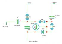
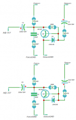
My mistake, i followed the LV No-Noise schematic for the Kelvin connections...please correct me if this one is not suitable.The negative with Kelvins shouldn't be like this?
You joined Force- and Sense-. Shouldn't they be separate?
I beleive that is interesting to use Kelvin connections if the D-Noiser is distant from the PSU Board.
*Optional 33R has been ad
Attachments
Last edited:
Thank Elvee..You don't need my approval since it is a completely open project, but I give it anyway
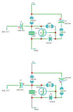
I added the 33R Optional D-Noizator: a magic active noise canceller to retrofit & upgrade any 317-based V.Reg.
PLEASE NOTE THIS PCB HAVE NOT BEEN TESTED YET...
I added the trace for 2SD2704 at the Bottom in case someone would like to test the board to replace the BC337
For fun I tried to use the 2SD2704 (a mute transistor with very high gain). In my simulation it performed very well, with a lower noise than the FZT851.
Attachments
Last edited:
- Home
- Amplifiers
- Power Supplies
- D-Noizator: a magic active noise canceller to retrofit & upgrade any 317-based V.Reg.