I have done it here:I do not fully understand this. Can you please draw this?
But you should carefully reread the whole thread to fully understand the requirements and implicationsFollowing a question, here is the schematic with some details shown explicitly, in particular the Kelvin connection:
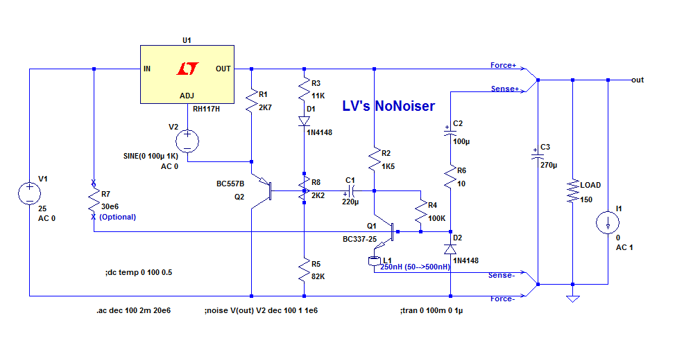
The input has no Kelvin connection, but it needs to be floating (separate) from the output connections, otherwise you will bypass the Kelvin connections, with unpredictable results because they will depend on the impedances of the concurrent pathsBut how can you make Kelvin connections on the input? How can you separate the input ground from output ground?
The LT317 is basically a 3-terminal device, with a common ground for both input and output, so how can I "separate them" ?
The most realistic option is to add a denoiser to the final regulator, preferably in a "pseudo-kelvin" connection, ie with the sensing terminals (with the the small arrows) directly connected to the point of load.So now I am wondering about bettering that small circuit, in hope of achieving even better sound.
Note that nonoiser or not, adding more than 2V dropout to an existing regulator is not necessarily a good idea: it will force the 317 into working with a minimal headroom, and you could even have the 100Hz ripple breaking in at times when your mains is low.
The denoiser alone will not suffer this potential problem
This is the reason I said that the nonoiser cannot be retrofitted: like any really high-perf regulator, it requires a thoughtful management of the grounds and supplies and Kelvin connections.The thing that worries me is the statement regarding "Kelvin Sensing". The modified CD Transport basically uses a common ground throughout.
Although, I could do the Kelvin Sensing within the independent low noise power source that I built for the off-board low jitter clock. Hmmm...
It has to be planned and built from scratch.
If you try to implement it in an existing equipment, there will be many obstacles like common grounds, etc.
Many kind thanks for your inputs. I need to dig through the rest of the thread (still working on it).I have done it here: ...
But from what you write I see that I can fully implement this circuit for the low noise voltage regulator (fed from separate floating supply), that I have feeding the external low jitter clock.
That alone should make a nice difference.
...
Comming back to the "global ground plane" problem, as typical in commercial audio equipment, I started fuzzy wondering, if it would be possible to "cascode" the global power supply, by means of using an add-on external low noise voltage reference.
As in "fooling" the existing device and its global ground plane by inserting a "cuckoo's egg" sideways supply.
As in: use the *existing* noisy power supply that be, but augment it, add, a low noise, low power sidebar supply, that will, by means of the NoNoiser, "modulate" the noisy power supply that be, together with its noisy global ground plane that be, ... into silence. Using the Kelvin Sensing at the legs of the specific critical chip that we want to provide with a clean supply.
I'm just thinking out loud, not sure yet where these thoughts are going. Probably nowhere.
Can the circuit as presented from you post be supplied from two independent power sources? A dirty one and a clean one?
The dirty one bearing the burden of the heavy duty currents,
and the clean one - providing but only a "cleaning delta" to the former?
Or asking differently: a way of "adding" a "cleaning delta" to an existing commercial device, or more specifically, to some of its important chips, a device with typical global ground plane, by means of a small "extra" added to the circuit, but in a manner that would require minimal interference / wreckage of the original PCB of the device?
Thrusting an add-on "delta" onto the pins of the critical chip. A delta that would void and null the noise that is happily wandering around the original commercial device.
For sake of discussion, let us assume that there is a wire jumper on the track that provides the rail voltage(s) to the chip. This wire jumper could be lifted and replaced with "something else" (resistor? inductor?), as a means of "measuring the noise" on that rail.
Last edited:
Not very clear, but if you try to force currents into the global (common) ground to please one supply load, say the +15V, this modulation will look like additional noise for other rails, like -15V, +3.3V, etc.e.
...
Comming back to the "global ground plane" problem, as typical in commercial audio equipment, I started fuzzy wondering, if it would be possible to "cascode" the global power supply, by means of using an add-on external low noise voltage reference.
As in "fooling" the existing device and its global ground plane by inserting a "cuckoo's egg" sideways supply.
If you attempt to treat more than one supply, the "correctors" will fight against each other, and they will all be losers
That is more less what I was suggesting by using "pseudo-kelvin" connections, but the effect is not going to be the same as true Kelvin+floating input sources: the power return currents will inevitably mess up thingsAs in: use the *existing* noisy power supply that be, but augment it, add, a low noise, low power sidebar supply, that will, by means of the NoNoiser, "modulate" the noisy power supply that be, together with its noisy global ground plane that be, ... into silence. Using the Kelvin Sensing at the legs of the specific critical chip that we want to provide with a clean supply.
If I interpret correctly what you mean, it would be something like the current-dumping scheme of Quad amplifiers, and the correction principle is general, not limited to 4-quadrants devices like an audio amp, meaning it could also work for a 1-quadrant device, but here again retrofitting is mission-impossible, and even if it is designed from scratch, it is not going to be simple and easyCan the circuit as presented from you post be supplied from two independent power sources? A dirty one and a clean one?
The dirty one bearing the burden of the heavy duty currents,
and the clean one - providing but only a "cleaning delta" to the former?
Or asking differently: a way of "adding" a "cleaning delta" to an existing commercial device, or more specifically, to some of its important chips, a device with typical global ground plane, by means of a small "extra" added to the circuit, but in a manner that would require minimal interference / wreckage of the original PCB of the device?
Ripple-cancellers can do that, and have been in use for decades ("gyrators" for example), but they generally require additional dropout and have limitations of their own.For sake of discussion, let us assume that there is a wire jumper on the track that provides the rail voltage(s) to the chip. This wire jumper could be lifted and replaced with "something else" (resistor? inductor?), as a means of "measuring the noise" on that rail.
If your goal is an ultimately clean supply, you need to use a super-clean linear regulator, period. There are commercial chips doing that + various custom super-regs of varying performance
Short of that, you can use the nonoiser and similar "augmenting" schemes (see examples in #1), but they are "band-aid" solutions.
If you need (or want) the best, there is no substitute for a dedicated circuit installed in a dedicated environment
Yeah. I know. Not quite sure myself re what I am aiming at.Not very clear, ....
Just musings.
I love the way you pour buckets of cold water on my hot head.
Thank you for your inputs.
The thing you say about the "canceling" for a specific chip will mess up the voltage relationships for all other surrounding chips - that I did not consider.
Nor did I consider the "fighting correctors" issue.
One can go only 'so far' when modifying existing equipment.
And then, if one does not want to "wreck" the original pcb too much, then the potential/scope of mods is somewhat limited.
Either way .... If one wants to have it done properly, then most probably heavy ingress into / wreckage of the existing PCB will be unavoidable. It may even turn out to do better by doing the "whole thing" from scratch.
Yup.
Life is what happens to you whilst you are busy making other plans.
I have received a PM asking a question about this topic:
Even if the worst-case 5µA current is purely made of noise, the resulting noise voltage for a typical plain-vanilla LM317 regulator (without Cadj) will be ~0.05Ω*5µA=0.25µV in the audio range: completely negligible already, but with the denoiser or the nonoiser in action, it will be tens of dB lower
Since the answer could interest other people, I am going to address it here.Quick question :
Will adding a 1N5819 (against polarity faults) and a 18 V zener behind the DeNoiser or any LM regulator with 15 V out, give more noise ? They are for protection . The 18V zener is a sharp one , even at 1 uA it still gives arond 17,4 V (1N4746A) , so at 15 V out, it only leaks some tens of nA. The 1N5819 (schottky) will leak more, like 5uA!
Even if the worst-case 5µA current is purely made of noise, the resulting noise voltage for a typical plain-vanilla LM317 regulator (without Cadj) will be ~0.05Ω*5µA=0.25µV in the audio range: completely negligible already, but with the denoiser or the nonoiser in action, it will be tens of dB lower
^ Thanks LV .
When I see many of the very beautiful , professonally made PCB's here , I laugh a bit at the small copper paths in 35 to 70um copper. I go fully overboard with copper. For my HPamp I'm going to use (like on my preamp) > 1mm2 solid copper to and from the regulators . Ground even more ! Copper resistance is about 0,016 ohm/m (1mm2) , so for max of 5cm between the regulator and the amp that will be 0,0008 ohm with max current of 50 mA , is about 40uV of music modulated noise , with a DeNoiser or NoNoiser which has < 1 uV. Now I can see why kelvin connections are important to get the best results. But then again de -sence of the NoNoiser has a current too from the emitter of transistor1 , going through a small 35um copper path....
There is of course the resistance of solder joints , but the sense lines have these too. (I never use connectors) .And yes I realize that the wiring inside the IC/transistor package between the chip and the leads are hair thin copper/gold .
The beauty of the Kelvin scheme is that the resistance of the sense terminals is irrelevant (within reason): they could be 1 ohm each without affecting the operation.
Even the force terminals tolerate some resistance, not 1 ohm of course because of the excessive voltage drop, but ordinary wires are perfectly sufficient.
Even the force terminals tolerate some resistance, not 1 ohm of course because of the excessive voltage drop, but ordinary wires are perfectly sufficient.
So thin?^ Thanks LV .
When I see many of the very beautiful , professonally made PCB's here , I laugh a bit at the small copper paths in 35 to 70um copper. I go fully overboard with copper. For my HPamp I'm going to use (like on my preamp) > 1mm2 solid copper to and from the regulators . Ground even more ! Copper resistance is about 0,016 ohm/m (1mm2) , so for max of 5cm between the regulator and the amp that will be 0,0008 ohm with max current of 50 mA , is about 40uV of music modulated noise , with a DeNoiser or NoNoiser which has < 1 uV. Now I can see why kelvin connections are important to get the best results. But then again de -sence of the NoNoiser has a current too from the emitter of transistor1 , going through a small 35um copper path....
There is of course the resistance of solder joints , but the sense lines have these too. (I never use connectors) .And yes I realize that the wiring inside the IC/transistor package between the chip and the leads are hair thin copper/gold .
Why not something more substantial?
Płaskownik miedziany miedź 20 x 5 mm - 100cm 8442445695 - Allegro.pl
So thin?
Why not something more substantial?
Płaskownik miedziany miedź 20 x 5 mm - 100cm 8442445695 - Allegro.pl
^
")
Well , copper is cheap .
Instictively I use a lot of copper . You should see my poweramp !
It's just now with LV pointing out on this thread the importance for kevin connections to get high performance , that I went to look for the actual resistance of copper , and that even a 50 mA signal through 5 cm of 1mm2 copper already gives 40uV noise. (well not actual noise , but if L & R share the same ground ... ). 5 cm x 1 mm of 70 um copper track will up that to 560uV. A 24 bit step of a 5 Vpp signal is around 0,3uV.
While the DeNoiser doesn't need a kevin connection , I just redesigned my PCB to get the LM+DeNoiser closer to the opamps.

^
Well , copper is cheap .
Instictively I use a lot of copper . You should see my poweramp !
It's just now with LV pointing out on this thread the importance for kevin connections to get high performance , that I went to look for the actual resistance of copper , and that even a 50 mA signal through 5 cm of 1mm2 copper already gives 40uV noise. (well not actual noise , but if L & R share the same ground ... ). 5 cm x 1 mm of 70 um copper track will up that to 560uV. A 24 bit step of a 5 Vpp signal is around 0,3uV.
While the DeNoiser doesn't need a kevin connection , I just redesigned my PCB to get the LM+DeNoiser closer to the opamps.
Last edited:
You tell those guys:^
Well , copper is cheap .
Train delays because of UK cable thefts soar, says Network Rail - BBC News
G'day Guys,
I am looking at using the denoiser for a preamp PSU.
The idea here is a +/-15v power supply PCB that is sufficiently modular that it could be readily adapted to other voltages. LM317/LM337 regs, BC337/BC327 transistors.
Here is the schematic I have come up with the base the PCB off. I'm pretty sure I've done that right but I will submit this for feedback. Tomorrow I will start working on a PCB layout.
What am I missing? There's no connection to the base of the transistors Q1 & Q2.
Yes there is. You can draw horizontally through a transistor (typically for parallelled bases though, here its to avoid having to reverse the symbols or redraw the layout)
There is a wiring error in the vicinity of Q1. It is not doing anything useful.G'day Guys,
I am looking at using the denoiser for a preamp PSU.
The idea here is a +/-15v power supply PCB that is sufficiently modular that it could be readily adapted to other voltages. LM317/LM337 regs, BC337/BC327 transistors.
Here is the schematic I have come up with the base the PCB off. I'm pretty sure I've done that right but I will submit this for feedback. Tomorrow I will start working on a PCB layout.
View attachment 790189
Missing connection between C9 and transistor.G'day Guys,
I am looking at using the denoiser for a preamp PSU.
The idea here is a +/-15v power supply PCB that is sufficiently modular that it could be readily adapted to other voltages. LM317/LM337 regs, BC337/BC327 transistors.
Here is the schematic I have come up with the base the PCB off. I'm pretty sure I've done that right but I will submit this for feedback. Tomorrow I will start working on a PCB layout.
View attachment 790189
- Home
- Amplifiers
- Power Supplies
- D-Noizator: a magic active noise canceller to retrofit & upgrade any 317-based V.Reg.