The Elektria concept first came to birth as an accessory in this project:
https://www.diyaudio.com/forums/tubes-valves/327831-supply-center-testing-tube-projects.html
I needed a low-power, variable supply to be used mainly as a bias source or for other secondary tasks.
As I found usual solutions unsatisfactory for various reasons, I brewed my own 0-100V regulator.
I came up with a Rush cascode as error amplifier, directly driving the ballast transistor.
This configuration offers lots of advantages: simplicity, no need to generate a tail current, capability to reach zero volt output easily, no need for auxiliary supplies and capability to regulate with less than 1V dropout.
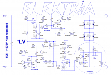
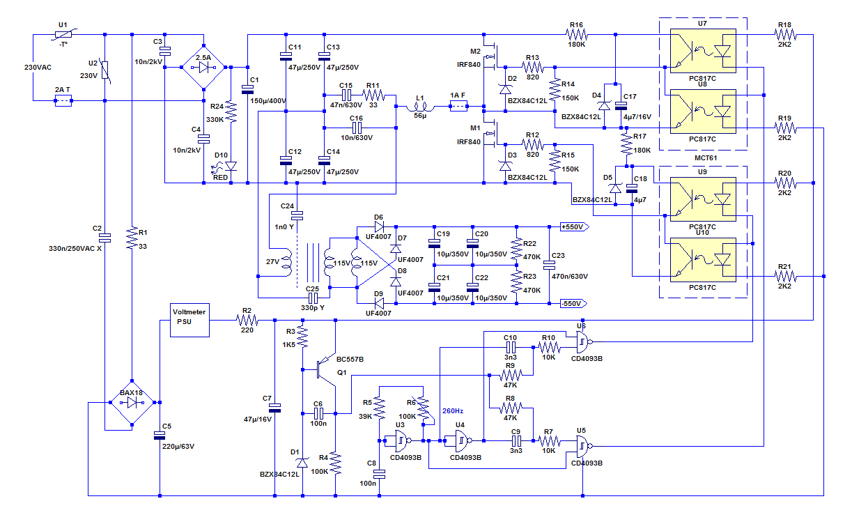
I was so pleased with the concept that I decided to test it in a standalone instrument: a 0-500V, 0-200mA.
For this proof of concept, I deliberately pushed the envelope to the limits: for example, the supply regulates 500V using mostly 300V transistors.
Not something I particularly recommend, but it demonstrates that it can be done.
The sensible solution would be to add cascodes of course.
Elektria is robust, stable and well-behaved, and its performances are good, but it cannot match the stability and regulation of a conventional, opamp-based regulator.
However, the performances are sufficient for at least 99% of tube-related DIY, and it has all the basic features of a lab supply: voltage and current can be freely adjusted between 0 and the maximum, a LED indicates when the current limitation is active, and it is equipped with a standby switch.
It is remarkably cost-effective, and can be built for practically any combination of voltage and current with minimal adaptations.
https://www.diyaudio.com/forums/tubes-valves/327831-supply-center-testing-tube-projects.html
I needed a low-power, variable supply to be used mainly as a bias source or for other secondary tasks.
As I found usual solutions unsatisfactory for various reasons, I brewed my own 0-100V regulator.
I came up with a Rush cascode as error amplifier, directly driving the ballast transistor.
This configuration offers lots of advantages: simplicity, no need to generate a tail current, capability to reach zero volt output easily, no need for auxiliary supplies and capability to regulate with less than 1V dropout.
I was so pleased with the concept that I decided to test it in a standalone instrument: a 0-500V, 0-200mA.
For this proof of concept, I deliberately pushed the envelope to the limits: for example, the supply regulates 500V using mostly 300V transistors.
Not something I particularly recommend, but it demonstrates that it can be done.
The sensible solution would be to add cascodes of course.
Elektria is robust, stable and well-behaved, and its performances are good, but it cannot match the stability and regulation of a conventional, opamp-based regulator.
However, the performances are sufficient for at least 99% of tube-related DIY, and it has all the basic features of a lab supply: voltage and current can be freely adjusted between 0 and the maximum, a LED indicates when the current limitation is active, and it is equipped with a standby switch.
It is remarkably cost-effective, and can be built for practically any combination of voltage and current with minimal adaptations.
Attachments
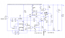
The Rush cascode (Q3 and Q4) is at the hearth of the circuit and constitutes its main strength: it is the source of all its unusual and desirable features.
However, in a Yin/Yang fashion, it is also its main weakness: the Rush circuit has an inherent 2Vbe offset between its inputs.
This means that some form of compensation is necessary; here, this task is carried out by D5 and D6: they shift the reference input by ~2Vbe.
However, this kind of compensation cannot be compared with the matching inherent in the classical LTP: in a LTP, the two junctions are identical, and operate at a similar current density.
Here, two diodes compensate for transistors, one NPN and one PNP.
This is a crude, first order compensation, certainly not suited for processing mV-level signals.
In a high-voltage supply though, the reference voltage can be made as high as practical: 33V in this case, because it is the practical limit imposed by integrated references, a TL431 here and a varicap regulator in the first version.
With a reference voltage ~30x the offset voltage, mismatches are reduced in the same proportion: for example, a 3% mismatch has a final impact of 0.1% on the output voltage.
This means that the thermal stability is not perfectly ideal, but it is more than adequate for most practical applications.
It would of course be possible to improve the situation, by using matched transistors in the cascode and its compensations for example, but I wanted to keep things as simple as practical.
I will discuss later ways of improving the basic circuit.
Also note that by swapping the inputs and using a common drain ballast, it is possible to build a more traditional-looking supply, but then you lose most of the advantages like LDO operation, etc.
It could however be advantageous for ultra-high voltage supplies: the ballast and the N-polarity member of the Rush pair can then be tubes.
With a Rush cascode, there is no externally defined tail current (and the "tail" node is not externally connected): the current is determined by the inputs, and during transients, it could become ~unlimited, which is why it is necessary to include a resistor, R15, to limit the current when the MOS gate voltage exceeds the 12V zener.
R15 also plays a role in the current limitation circuit, and in reducing the working voltage seen by Q3 to <300V.
This resistor is bypassed by a small capacitor to eliminate the parasitic pole that it creates.
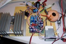
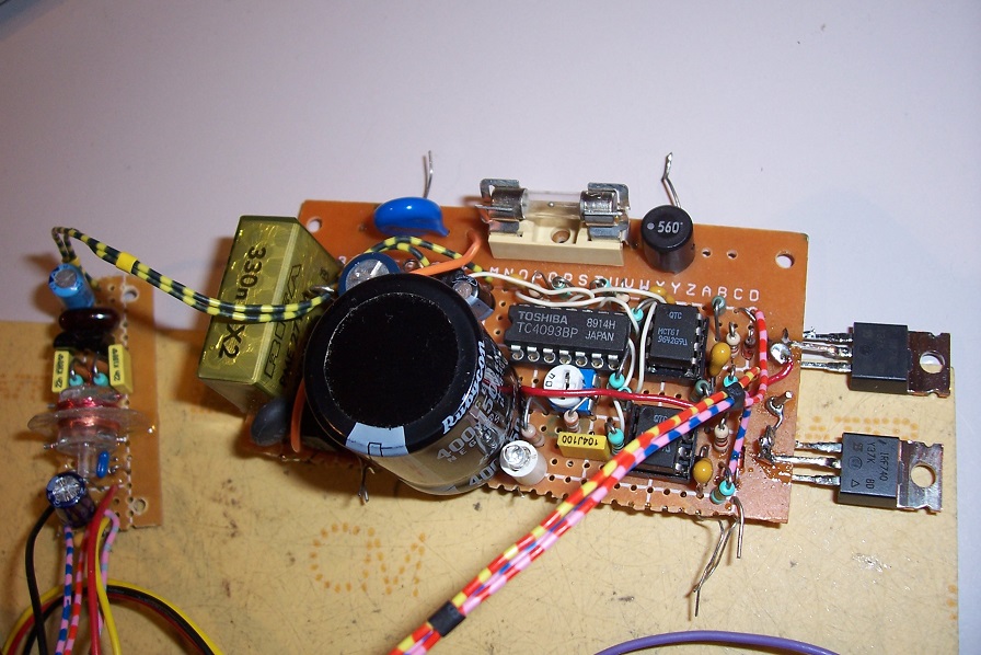
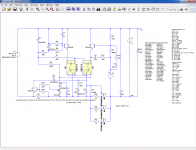
Here is a pic of the regulator module: only its lower section is dedicated to the actual linear regulator:
However, in a Yin/Yang fashion, it is also its main weakness: the Rush circuit has an inherent 2Vbe offset between its inputs.
This means that some form of compensation is necessary; here, this task is carried out by D5 and D6: they shift the reference input by ~2Vbe.
However, this kind of compensation cannot be compared with the matching inherent in the classical LTP: in a LTP, the two junctions are identical, and operate at a similar current density.
Here, two diodes compensate for transistors, one NPN and one PNP.
This is a crude, first order compensation, certainly not suited for processing mV-level signals.
In a high-voltage supply though, the reference voltage can be made as high as practical: 33V in this case, because it is the practical limit imposed by integrated references, a TL431 here and a varicap regulator in the first version.
With a reference voltage ~30x the offset voltage, mismatches are reduced in the same proportion: for example, a 3% mismatch has a final impact of 0.1% on the output voltage.
This means that the thermal stability is not perfectly ideal, but it is more than adequate for most practical applications.
It would of course be possible to improve the situation, by using matched transistors in the cascode and its compensations for example, but I wanted to keep things as simple as practical.
I will discuss later ways of improving the basic circuit.
Also note that by swapping the inputs and using a common drain ballast, it is possible to build a more traditional-looking supply, but then you lose most of the advantages like LDO operation, etc.
It could however be advantageous for ultra-high voltage supplies: the ballast and the N-polarity member of the Rush pair can then be tubes.
With a Rush cascode, there is no externally defined tail current (and the "tail" node is not externally connected): the current is determined by the inputs, and during transients, it could become ~unlimited, which is why it is necessary to include a resistor, R15, to limit the current when the MOS gate voltage exceeds the 12V zener.
R15 also plays a role in the current limitation circuit, and in reducing the working voltage seen by Q3 to <300V.
This resistor is bypassed by a small capacitor to eliminate the parasitic pole that it creates.
Here is a pic of the regulator module: only its lower section is dedicated to the actual linear regulator:
Attachments
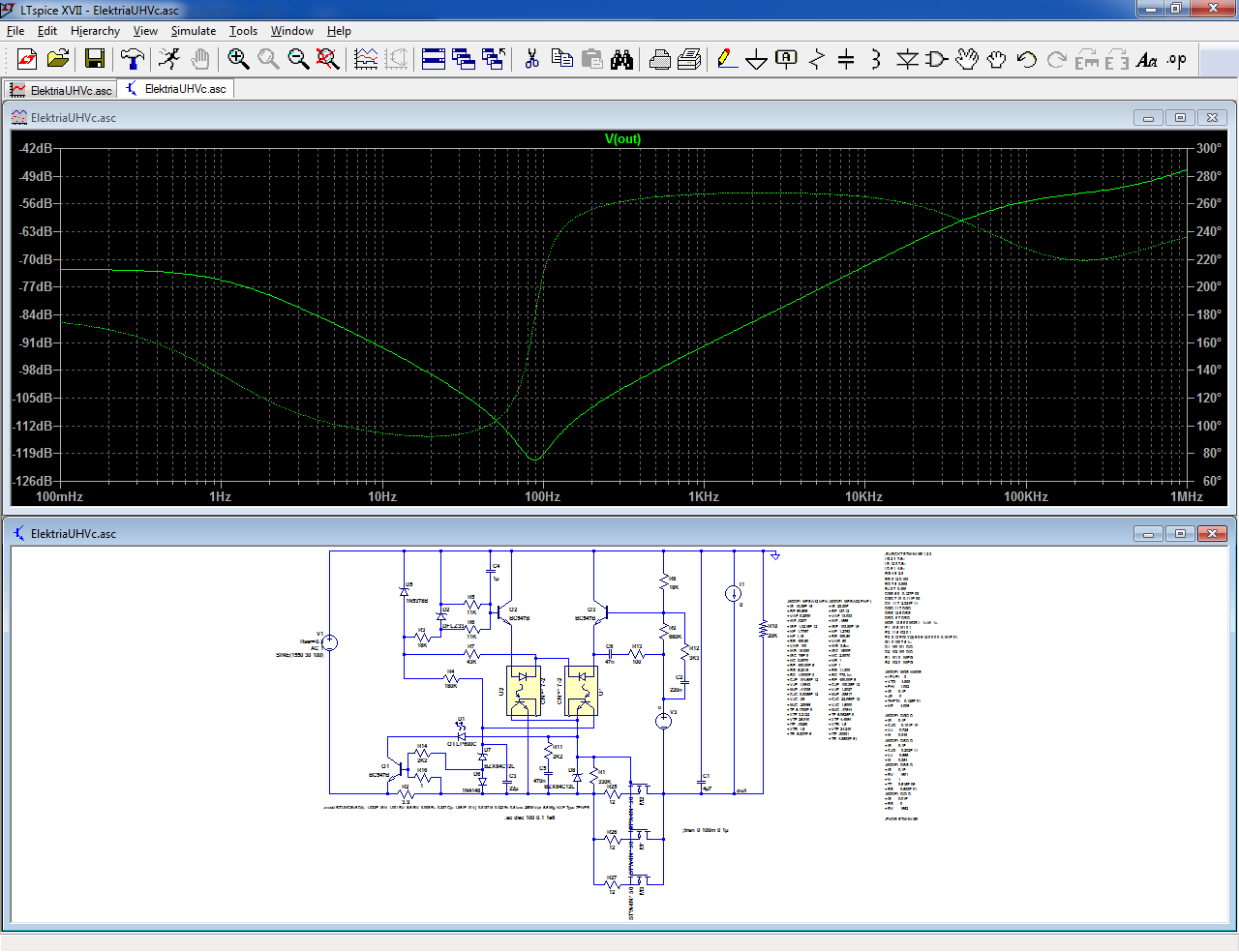
Here are some (indicative) performance curves: for most of the audio frequency range, the output impedance remains at ~30mΩ and the PSRR at -76dB.
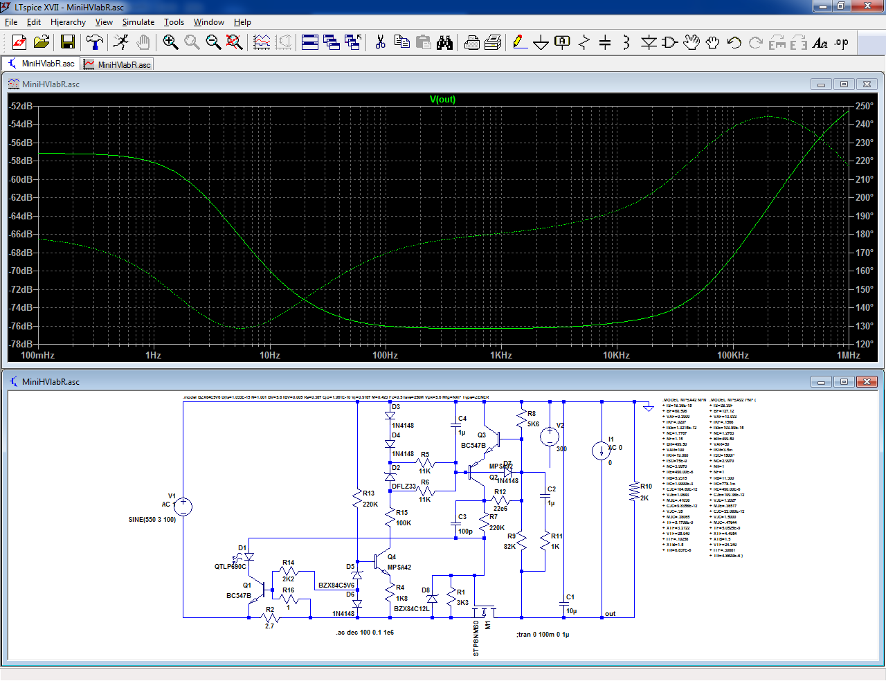
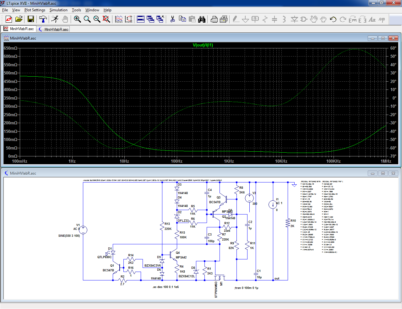
As I warned, this is not phenomenal: some super-regulators presented by community members boast < µΩ output impedance and < -140dB PSRR, but here the scope is different, as are the means: after all, the complete regulator comprises just 4 transistors (the current limiting transistor does not affect the performances).
It is however perfectly sufficient for most of DIY work, and a simple discrete architecture tends to be more robust regarding mishaps and perturbation ingress than more complex ones using ICs for example.
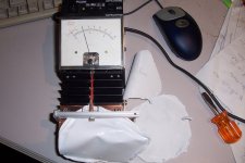
For this one-off, I made the choice of a single ballast transistor, fitted with a very large extruded heatsink.
Since the power dissipated can reach ~110W, ~half the max power capability of the MOSfet, I had to use a heat-spreader for the mounting: no TO247 insulated mounting method can come near what is required, and although the drain is almost at the -rail potential, I still wanted a good insulation: a lab supply can be used in situations where any rail can be at any potential, including AC.
This gave me the opportunity to use my own SILpad fab: this example is 0.3mm thick and has only 2°C.cm²/W thermal resistivity.
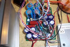
It is a test sample, composed of ordinary RTV121 and more than 50% of MgO:

As I warned, this is not phenomenal: some super-regulators presented by community members boast < µΩ output impedance and < -140dB PSRR, but here the scope is different, as are the means: after all, the complete regulator comprises just 4 transistors (the current limiting transistor does not affect the performances).
It is however perfectly sufficient for most of DIY work, and a simple discrete architecture tends to be more robust regarding mishaps and perturbation ingress than more complex ones using ICs for example.
For this one-off, I made the choice of a single ballast transistor, fitted with a very large extruded heatsink.
Since the power dissipated can reach ~110W, ~half the max power capability of the MOSfet, I had to use a heat-spreader for the mounting: no TO247 insulated mounting method can come near what is required, and although the drain is almost at the -rail potential, I still wanted a good insulation: a lab supply can be used in situations where any rail can be at any potential, including AC.
This gave me the opportunity to use my own SILpad fab: this example is 0.3mm thick and has only 2°C.cm²/W thermal resistivity.
It is a test sample, composed of ordinary RTV121 and more than 50% of MgO:
Attachments
Last edited:
The current-control section is not a true regulator but rather a current limitation made variable from zero to the maximum.
The current is not very accurately defined, and the output resistance in current mode is relatively high, but certainly not infinite.
The implementation could not be simpler: a single transistor Q2 sensing the voltage developed across the shunt R1, with a compensation by D2.
When it is active, the limitation shunts the G-S of the MOS, and the current shunted also illuminates the limitation indicator D4
Of course, the thermal compensation only becomes fully active when the current is set to zero.
As the current is increased, the compensation becomes progressively less effective.
This means that for high current settings, the limitation will have a negative tempco.
I didn't view that as an inconvenient: when the ambient temperature is high, the maximum current will be reduced which is helpful considering the dissipation possible in the ballast at the full current: up to 100~110W when the output is shorted.
This completes the description of the purely Elektria part of the schematic.
In my prototype, to make it usable, I have added some accessories and a mains front-end.
I will also describe them, but I do not not especially recommend building them.
The raw HV supply in particular is a bit quirky (but it works!).
The supply for the small LED panel-meter has already been described elsewhere:
Symetrical Colpitts oscillators
Here is the raw 550V supply, for the sake of completeness:
Ideally, I would recommend a pure traditional transformer supply, but even with the relatively modest output current I opted for, the required DC power input was ~130W, requiring a 200~250VA transformer having the correct secondary voltage, something I didn't have in my stash.
I resorted to a 25VA, 2x115V to 27V transformer I used backwards.
Of course, you cannot apply the brute 50Hz in those conditions, which is why I devised a simplistic converter (or frequency-changer) operating a little above 250Hz.
This respects V.s product of the core, and allows a higher power to be passed: firstly, because of the increased frequency, secondly because the PF of a rectifier working on squarewaves is ~unity, and thirdly because the power delivered by a squarewave does not fluctuate over time, allowing a 100% utilization factor of the transformer.
All of this means that the nominally 25VA transformer can in fact deliver a 130W DC output easily.
Of course, the increased frequency increases the iron losses, but at 260Hz and with a reduced induction, no additional temperature elevation is detectable under no-load conditions with this transformer (it could be different for other iron qualities).
Most of the circuit is pretty ordinary, except the MOS-driving section: the signals from the oscillator U3 have dead-times added by U5 and U6, and are transmitted to the gates through push-pull optocouplers fed directly from the voltage to be switched.
The scheme is very economical, and perfectly suited to the frequencies involved.
Attachments

Additional remarks:
The dead-times in the converter have two purposes: a very obvious one is to prevent any risk of cross-conduction and shoot-through currents in the MOS half-bridge.
The other is to let the transformer do the switching "naturally", to avoid the very fast edges the MOS themselves would generate.
The "primary" (former secondary in fact) is filtered and snubberized for the same reason.
The secondary rectification uses UF4007 diodes, which may look like overkill: in principle, below 400Hz, ordinary rectifiers should suffice, and initially I had used 1N4007's, but I noticed unwanted effects: due to the squarewave operation and the very low leakage inductance of the transformer, the diodes "sticking" for a few µs at each transition created violent current spikes, translating into ringing and perturbations.
Snubbers were of no help, in fact they made the matter worse.
Adding a saturable inductor in series with the winding did solve the problem, but just replacing the slow diodes by very fast ones was simpler and worked as nicely.
Because it is a lab supply (and I am going to actually use it as soon as it is boxed), I wanted it to be perfectly quiet.
In addition to the above, I also connected the transformer's electrostatic screen to the cold side of a primary (via a Y cap, for added safety).
I also connected a balancing capacitor C25 to one side of the secondary, to eliminate any common-mode switching residue.
Note that although this cap is of the Y variety for safety reasons, it isn't used as a regular Y cap: these caps are generally placed between the primary and secondary "colds", which is not the case here.
To achieve the same rejection effect with the "normal" connection, a much larger value, like 10 or 22nF would be required.
Regarding the main Elektria schematic, the role of Q5 and its associated components is to compensate the current consumption of various "parasitics", like the feedback divider, in the output ammeter.
Not something essential, but since I had an auxiliary supply available for the voltmeter module, I preferred to do things properly.
I am now going to look at (simple) possible ways of improving the basic circuit, but first, let us talk about Elektria's less visible (or invisible) attributes.
To construct a variable supply, you have two basic options: you can start with a fixed reference voltage, and use the regulator to multiply this reference by a variable factor in order to attain the target voltage. This factor is the closed-loop gain, and to manipulate it, the feedback factor is altered: that is exactly the way a LM317-type regulator works.
The other method is to vary the reference only, and keep all the rest constant.
In DIY work, both are in use, with a strong preference for the former though: think LM317, Maida, and the many likes...
Is one of the schemes superior to the other?
For a control-theory specialist, that's a no-brainer: acting on FB to modify the gain of the plant to arrive at the desired output is crap, non-sense, etc, only tolerable for fine-tuning when no other option is practical
With the gain control method, there is a first, obvious problem: the minimum gain being 1, the lowest output voltage reachable is the reference itself.
This could be annoying for low-voltage supplies, but at 300~500V, it is just an almost negligible detail.
Real problem are elsewhere: when you change the FB and gain in a closed-loop system, you also change everything else: output resistance, transient behavior, stability margins, static error, offset errors amplification, etc.
In a regular 317 application, the gain ratio required spans 25~30, which is already large, but at 500V, the ratio is 1:400: that's what I call extreme stretching.
With the reference control, all the parameters remain consistent, whatever the voltage setting.
That is the method used universally in serious, professional gear, and surprisingly, it is also used in Elektria.
This means for example that you can make PSRR tests by superimposing a modulation to the ref. voltage: the result will be consistent and predictable.
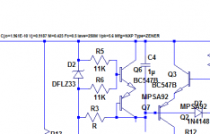
To improve the Rush compensation, a first option is to replace the compensating diodes by transistors identical to the Rush:
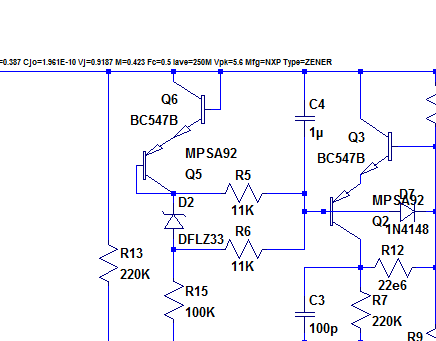
A problem with this approach is that the transistors do not work in the same conditions as those they mimick, making the compensation non-ideal.
A better solution is to connect the NPN as a follower and the PNP as a diode:

The compensation can be fine-tuned by adjusting the current in R3.
Unfortunately, the follower ends up where it is the least needed: to optimize the OL gain and increase the FB divider's values, it would be preferable to buffer this input, but that is not practical: both inputs would end up shifted wrt. GND, and driving Q3 would be almost impossible without an auxiliary supply
To construct a variable supply, you have two basic options: you can start with a fixed reference voltage, and use the regulator to multiply this reference by a variable factor in order to attain the target voltage. This factor is the closed-loop gain, and to manipulate it, the feedback factor is altered: that is exactly the way a LM317-type regulator works.
The other method is to vary the reference only, and keep all the rest constant.
In DIY work, both are in use, with a strong preference for the former though: think LM317, Maida, and the many likes...
Is one of the schemes superior to the other?
For a control-theory specialist, that's a no-brainer: acting on FB to modify the gain of the plant to arrive at the desired output is crap, non-sense, etc, only tolerable for fine-tuning when no other option is practical
With the gain control method, there is a first, obvious problem: the minimum gain being 1, the lowest output voltage reachable is the reference itself.
This could be annoying for low-voltage supplies, but at 300~500V, it is just an almost negligible detail.
Real problem are elsewhere: when you change the FB and gain in a closed-loop system, you also change everything else: output resistance, transient behavior, stability margins, static error, offset errors amplification, etc.
In a regular 317 application, the gain ratio required spans 25~30, which is already large, but at 500V, the ratio is 1:400: that's what I call extreme stretching.
With the reference control, all the parameters remain consistent, whatever the voltage setting.
That is the method used universally in serious, professional gear, and surprisingly, it is also used in Elektria.
This means for example that you can make PSRR tests by superimposing a modulation to the ref. voltage: the result will be consistent and predictable.
To improve the Rush compensation, a first option is to replace the compensating diodes by transistors identical to the Rush:
A problem with this approach is that the transistors do not work in the same conditions as those they mimick, making the compensation non-ideal.
A better solution is to connect the NPN as a follower and the PNP as a diode:
The compensation can be fine-tuned by adjusting the current in R3.
Unfortunately, the follower ends up where it is the least needed: to optimize the OL gain and increase the FB divider's values, it would be preferable to buffer this input, but that is not practical: both inputs would end up shifted wrt. GND, and driving Q3 would be almost impossible without an auxiliary supply
Attachments

This is superb dear! Congratulations! I will probably build it during Christmas vacations. Would it be possible to upscale Voltage to say 1300v (with normal transformers of course) by fet cascading with lets say 4 power fets and some adaptation to the rest of the circuit and range between 200-1300 ? Sounds crazy I know....
Last edited:
NMOS FETs can do >1300V without the need for cascoding, so no problem there (you can parallel them for higher power).
For the PNP drivers, reusing the same kind of resistor trick as I did is not possible for 1300V (not realistic anyway), so 3 to 5 cascode stages would be required, but that shouldn't be a problem, because MPSA92's are incredibly cheap, their quality doesn't matter (most of the semi's of my build are just cheap chinese copies), and the number of cascodes will not affect in any way the performances.
BTW, why limit yourself to 200V as a low limit? Going to zero costs nothing, and even if you think you won't need it 99% of the times, the 1% will come and bite you at some point in the future.
I will post a schematic adapted for voltages up to 1.5kV in the next few days.
Welcome to the Elektr⚡a club!
Hi Elvee
In #3, you shown the results of making of your own Silpad rubber from RTV and magnesium oxide powder. That suggests you have access to industrial raw materials, suitable platens for pressing the mass to a controlled thickness and a blending system for the powder that gives excellent dispersion. Is there no end to your talents and breadth of industry knowledge?
I have a question about the platen surface though; how did you ensure the RTV would release easily, since 0.3mm or less would be quite weak when extended with powdered fillers?
Not anymore: I am retired, and I have to use "improvised" techniques, clamps, shims, vice, etc.Hi Elvee
In #3, you shown the results of making of your own Silpad rubber from RTV and magnesium oxide powder. That suggests you have access to industrial raw materials, suitable platens for pressing the mass to a controlled thickness and a blending system for the powder that gives excellent dispersion.
I have found a number of suppliers, both on line and physical, and sometimes I also buy from a pharmacy: it is expensive, but for small quantities it remains bearable, and the purity of the products is much better than for industrial-grade ones.
That's where my MgO came from: this 250g jar cost me ~50€ IIRC.
Not cheap, but acceptable.
The blending part is the most difficult (for me): to achieve low thermal resistivity, the proportion of filler must be as high as possible, but the mix becomes so dry, chalky and flaky as to make it impossible to work with.
The workaround I found was to add a volatile solvent during the mixing phase, and then let it evaporate before the final pressing.
The RTV I used is a two-component used for modelling, moulding, etc.I have a question about the platen surface though; how did you ensure the RTV would release easily, since 0.3mm or less would be quite weak when extended with powdered fillers?
It does not naturally adhere much to surfaces, unlike sealant-type ones.
Anyway, I coat the pressing surfaces with polypropylene industrial tape.
I generally include a small proportion or a veil of fiber glass to reinforce the product, but for this one I didn't: it makes it more fragile (but still perfectly manageable), but also more supple, deformable and adaptable to the surfaces
Attachments

NMOS FETs can do >1300V without the need for cascoding, so no problem there (you can parallel them for higher power).
For the PNP drivers, reusing the same kind of resistor trick as I did is not possible for 1300V (not realistic anyway), so 3 to 5 cascode stages would be required, but that shouldn't be a problem, because MPSA92's are incredibly cheap, their quality doesn't matter (most of the semi's of my build are just cheap chinese copies), and the number of cascodes will not affect in any way the performances.
BTW, why limit yourself to 200V as a low limit? Going to zero costs nothing, and even if you think you won't need it 99% of the times, the 1% will come and bite you at some point in the future.
I will post a schematic adapted for voltages up to 1.5kV in the next few days.
Welcome to the Elektr⚡a club!
What can I say? Superb ! Thank u!
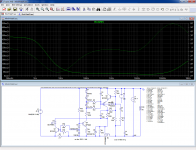
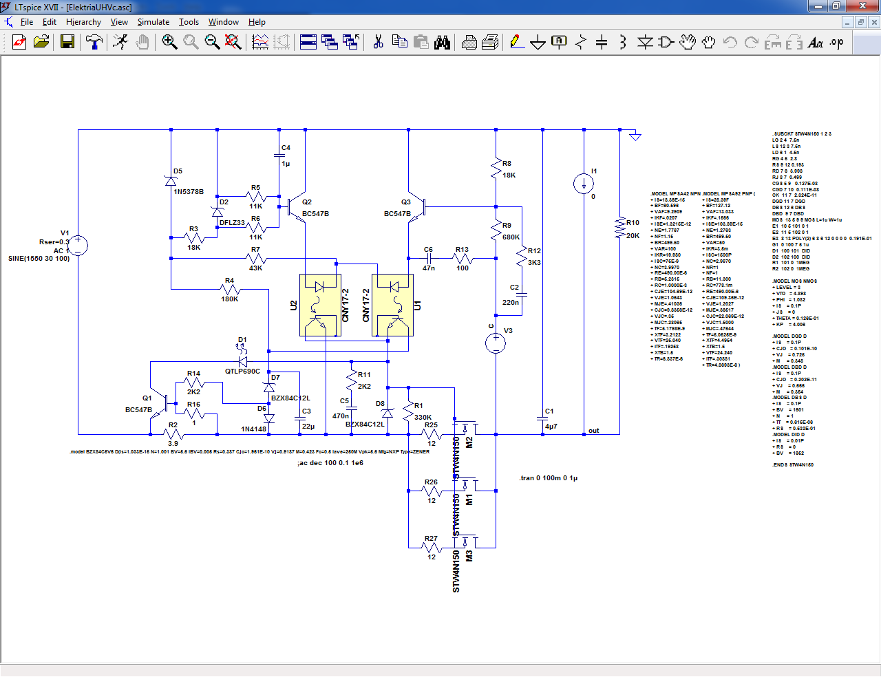
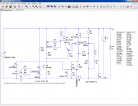
Here is a first draft.
Assumptions are 1300V output max, 150mA max output current.
This may seem low, but with such a voltage it already represents ~200W, and an almost unlimited of parallel MOSFETs can be added if required.
The sim uses 1500V types from ST, because they don't have a spice model for their 1700V part, but other manufacturers also have HV devices.
This example is just an extrapolation of the base Elektria circuit, but because of the extreme voltage, other options are worth considering.
I will explore some of them later.
Attachments
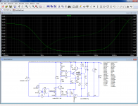
Here is another possibility: the CCS string is replaced by a 100V shunt regulator, saving a few transistors and simplifying the circuit a little bit.
The PNP signal string is still required though.
I will also examine more radical variants, using alternative voltage-translation techniques.
Note that all these drafts are just for simulation purpose, and need additions and refinements before they can be used in reality.
The PNP signal string is still required though.
I will also examine more radical variants, using alternative voltage-translation techniques.
Note that all these drafts are just for simulation purpose, and need additions and refinements before they can be used in reality.
Attachments
In this variant, the voltage-translation task is carried out by opto-couplers.
Does this avatar still belong to the Elektria family, without the emblematic Rush error amplifier?
The question is open to debate, but it shares all of the family traits:
LDO capability, variation from zero to the max through a fixed multiplication of a variable reference, NMOS ballast referenced to the negative rail, error amplifier referenced to the positive rail, no auxiliary supply required, fully discrete and minimalistic, with decent performances.
The main advantage brought by this topology is an effortless voltage translation, independent of the voltage level.
Additionally, both inputs are now referenced to the +rail, with no need to compensate a 2.Vbe offset.
Optocouplers have some peculiarities: in this implementation, they provide a huge DC gain, but the frequency characteristics of standard opto's is rather poor, and taken together, these characteristics impose a very heavy-handed approach to the frequency-compensation strategy.
The dominant pole is provided by C5, the shunt compensation.
Additional corrections are provided by C6.
More creative schemes could in principle make better use of the raw gain available, and I tried an active compensation but it had issues, and even more complication would be required.
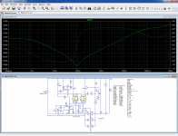
However, even with a plain-vanilla compensation this topology remains quite effective, as the PSRR curve shows:
Optocouplers are not famed for their stability and consistency, but here they are inside the control loop, and they are paired, thus minimizing the effect of drift and dispersion.
It is possible to use a dual type, like the MCT61 to improve tracking.
Does this avatar still belong to the Elektria family, without the emblematic Rush error amplifier?
The question is open to debate, but it shares all of the family traits:
LDO capability, variation from zero to the max through a fixed multiplication of a variable reference, NMOS ballast referenced to the negative rail, error amplifier referenced to the positive rail, no auxiliary supply required, fully discrete and minimalistic, with decent performances.
The main advantage brought by this topology is an effortless voltage translation, independent of the voltage level.
Additionally, both inputs are now referenced to the +rail, with no need to compensate a 2.Vbe offset.
Optocouplers have some peculiarities: in this implementation, they provide a huge DC gain, but the frequency characteristics of standard opto's is rather poor, and taken together, these characteristics impose a very heavy-handed approach to the frequency-compensation strategy.
The dominant pole is provided by C5, the shunt compensation.
Additional corrections are provided by C6.
More creative schemes could in principle make better use of the raw gain available, and I tried an active compensation but it had issues, and even more complication would be required.
However, even with a plain-vanilla compensation this topology remains quite effective, as the PSRR curve shows:
Optocouplers are not famed for their stability and consistency, but here they are inside the control loop, and they are paired, thus minimizing the effect of drift and dispersion.
It is possible to use a dual type, like the MCT61 to improve tracking.
Attachments
Back to the Rush configuration:
An interesting combination is a hybrid Rush, with one member bipolar and the other MOS.
It makes the use of a compensating MOS follower in the reference arm compulsory, but it brings two key advantages: both inputs are now ground referenced (and include the ground in their CM range, of course), and the feedback input has a much larger impedance, allowing larger resistor values in the feedback divider (R8 and R9).
Not something to be scorned at for output voltages >1kV
Panos, I think that you now have a large enough gamut to chose from.
Which one would you like to see developed?
What are your requirements (output current...) and your preferences regarding components (MOSfets source...)?
A word of caution: whatever your choice is, this is not a project to be taken lightly: the voltage and power level are more than lethal, and HV circuits always have nasty surprises in store for the beginner or the unwary.
You should not start such a project without prior experience in seriously high voltages.
The usual 400~500V of ordinary tube circuits is one thing, power circuits operating at >1kV are something completely different.
Attachments
The weakest aspect of Elektria is her current handling: it is more a variable limitation than a true current regulator; for 99.9% of tube work, this is perfectly sufficient (which is why I chose to implement it in that simplistic manner), but some may prefer a current control on a par with voltage.
It is possible without too much complication, basically one additional opamp, U1.
The type doesn't matter very much, it just needs to include the -V rail in its common mode range.
The LT1013 fits the bill, as does the LM358 and many others.
The discrete limitation transistor is left in place, because opamps are not particularly fast, especially when they have to wake up from a saturated state, and the transistor provides a feedforward path, bypassing the opamp in case of a brutal short of the output.
Elektria is essentially a current generator, but the short and fast voltage FB path perfectly emulates a voltage generator, which is why it is preferable to include this (cheap) safety measure.
Most of the variations described so far can be mixed and blended with one another to suit particular needs.
Attachments
Dearest Elvee,
I am really astonished for all this excellent work of yours and the time spent for my request!
My requirement is a voltage regulator for testing various amplifiers with big transmitting tubes like 450TL, 4-400, etc. My main amp is a (450TL in SE).
So i Need a an adjustable power supply to replace my current variac-HV transformer - rectifier compo used till then.
My requirements is reliability, adjustability, and fairly immune to short circuiting just in case... I know how ugly a 1Kv short looks! Nice frequency response and low output impdance would be nice too. I think a variation between thw CCS schematic and the one with the OPAMP would fit the bill...
Thanks again,
Panos
My power requirement is about 150-200mA max and range from lets say 100-1500 absolute max.
I have a lot of these mpsa transistors and a lot of 2sk1120, VNS008A and IRF450s.
Back to the Rush configuration:
An interesting combination is a hybrid Rush, with one member bipolar and the other MOS.
It makes the use of a compensating MOS follower in the reference arm compulsory, but it brings two key advantages: both inputs are now ground referenced (and include the ground in their CM range, of course), and the feedback input has a much larger impedance, allowing larger resistor values in the feedback divider (R8 and R9).
Not something to be scorned at for output voltages >1kV
Panos, I think that you now have a large enough gamut to chose from.
Which one would you like to see developed?
What are your requirements (output current...) and your preferences regarding components (MOSfets source...)?
A word of caution: whatever your choice is, this is not a project to be taken lightly: the voltage and power level are more than lethal, and HV circuits always have nasty surprises in store for the beginner or the unwary.
You should not start such a project without prior experience in seriously high voltages.
The usual 400~500V of ordinary tube circuits is one thing, power circuits operating at >1kV are something completely different.
As I said earlier, raw performances and exceptional figures aren't the main design goals of this supply: performances are more than decent and should be ample enough to meaningfully test most of the tube designs, but with its 3~4 discretes, it cannot rival IC-intensive alternatives.Nice frequency response and low output impdance would be nice too.
On the plus side, this brings advantages like robustness and sanity (=absence of complex pathological behaviors) and ease of sourcing commodity components.
I will propose a suitable topology, and I will explore the dimensioning in some details to let you and other members tailor their supply to their needsI think a variation between thw CCS schematic and the one with the OPAMP would fit the bill...
Regarding the pass transistor(s), it would be preferable to use a type able to withstand the full input voltage, in parallel combination for higher dissipation.My power requirement is about 150-200mA max and range from lets say 100-1500 absolute max.
I have a lot of these mpsa transistors and a lot of 2sk1120, VNS008A and IRF450s.
Ixys, ST, etc have suitable HV types.
It is in principle possible to use a series cascade (and I am aware this would be more advantageous in your case), but it is less safe and robust than paralleling, especially at this voltage level.
In addition, I have only tested parallel combinations in real-world.
I can explore the series possibility in sim, but a sim is just that, and the reality test could be disappointing, especially for extra-high voltages.
That said, if you have heaps of 2SK1120's and you are prepared for a number of possibly unsuccessful tests, why not give it a try?
- Status
- This old topic is closed. If you want to reopen this topic, contact a moderator using the "Report Post" button.
- Home
- Amplifiers
- Power Supplies
- ELEKTR⚡A is a true High-Voltage lab supply, truly DIY-friendly