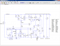
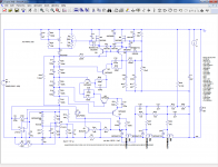
Here is a first, provisional (and non-functional) draft.
It shows the main options retained, but is not adapted yet to the ~1.7kV input.
I have used the hybrid MOS/Bjt Rush for mainly one reason: it has high input impedances.
This in turn allows higher resistor values in the FB divider and the reference input.
This is important, because at 1.7kV, each mA consumed translates into almost 2W of heat.
I know that for a big tube amps lover, it is a mere detail, but it is not a reason to overindulge.
The two small MOS will preferably be matched, but that is not a huge burden.
To reduce the current consumption, one could think of reducing the current in the "spine" of the Rush, but this would reduce the GBW product because of the large capacitance of HV MOS.
Because of the high voltage, I have discarded the N cascade string and replaced it by shunt regulators for both the high and low sides.
The dissipation is the same, but it requires much less components for this voltage.
The P cascade will still be required
The low-side regulator looks somewhat insane: the spare opamp regulates its own supply.
Because suitable opamp for the current regulation come in duals (LT1013, LM358,...), it is a good way to use the spare operator.
Despite being unusual, this configuration offers extremely high performances, and it is proven: I have been using it for many years
Attachments
That is so nice! I am already trying to schedule how the pcb should be with the voltage requirement under consideration. Can you please post the tl431 model you are using as well as the complete acs if I am not asking too much. I would love to play around with this on ltspice!
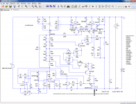
Here is the next stage:

The main change is the inclusion of the voltage translating cascodes and their reference divider.
A total of 5 MPSA92's share the voltage. This could seem insufficient, but part of the voltage is taken up by the series resistors: ~200V for the transistors, and 200V for each 100K resistor, thus 400V/stage, which leaves a comfortable margin.
Note that during transient conditions, the "spine" current could fall to zero, meaning the transistors would see ~350V, which is principle too much and would drive them into avalanche, but here the current is severely limited, and the transistors are surrounded by 100K resistors, meaning the avalanche regime is not dangerous and is completely reversible.
The bias string beginning with R26, 27,.. also serves to bias the two shunt regulators: they need a little under 2mA to operate, which determines the total value.
R26 is smaller than the other four, because 133V are taken up by the high-side shunt reg.
R34 is added to avoid E24 values in the string: nominally they should be 110K, 160K.
The total no-load input current with the max. output voltage of 1500V is ~4.5mA, which could seem remarkably frugal, until you realize that at 1700V, it already represents ~8W.
It is certainly better and simpler than having to add two auxiliary supplies, requiring a special insulation for 2kV.
Talking about insulation, both the current and the voltage pots need to be well insulated from everything else: they sit 1.7kV apart, and depending on how the supply is used, they could be brought at a high potential wrt. the ground or chassis of the DUT.
Some of the protections have also been added, the compensations have been adapted, and the supply is now dimensioned for an output of 1500V/200mA, and it operates in sim.
The next important step will be the addition of a proper ballast
Attachments
The simplest, most straightforward and therefore safest method of adapting the ballast to a ~1.7kV input is to use a MOSFET capable of withstanding such a voltage.
Fortunately, such devices are now available, mainly from Ixys.
Other alternatives exist: from ST or Cree (SiC), but at the moment their top voltage seems to reach just 1.7kV.
They are probably usable, but the exercise would be somewhat acrobatic.
At the moment, even Ixys has a somewhat patchy range of voltage/current/power/Rdson combinations at this voltage level.
For these reasons, and the fact that a spice model is available, I opted for the IXTK5N250 as an example, a monster capable of dissipating 960W.
I used two in parallel, because asking a single transistor to dissipate 340W is completely insane (170W is just moderately insane).
Little more needs to be said: the change in characteristics does not seem to impact very much the sim compared to the 8A/600V from ST
Attachments
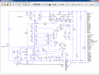
Here is the series ballast version: resistors R32, 35 and 36 share the dropped voltage equally between the three transistors, the minimum possible number for 600V or 800V devices.
Additional series or parallel devices might be needed for a sufficient dissipation.
C15, 21 and 22 ensure a correct dynamic sharing, something essential for a lab supply.
A 560V to 600V TVS or varistor connected across each transistor could also be helpful.
The role of R39 and R40 is to shift the gate voltages by a few volts, to cancel the threshold voltages of the series MOSFETs.
Without them, the dropout voltage could not go below ~2Vth, which is probably not hugely important for a 1500V supply, but adding them allows even this version of Elektria to remain in the LDO class.
The series version presents a unique problem: the resistive divider is connected to the output, but it is also referenced to the non-regulated input.
This means that it will bypass the ballast transistors, and inject a parasitic current into the output, about 0.5mA with the chosen values.
It will probably not be noticeable with most of the load/output voltage conditions, but it will impact the no-load output.
Two simple mitigations measures are possible: add a bleeder resistor to the output or increase the resistance of the divider.
The bleeder has obvious drawbacks, and increasing the divider very much is also going to pose problems, like sensitivity to leakage currents or electrostatic couplings.
It is probably possible to go much higher than 1 megohm without trouble, but how much exactly is not clear, and will heavily on the physical implementation.
A less simple remedy is to add a shunt member to the output: this would change the 1-quadrant supply into a 2-quadrant and would have other benefits regarding dynamic behavior, but with 1500V it is not going to be especially easy.
If someone has a better suggestion, I would warmly welcome it....
Attachments
Last edited:
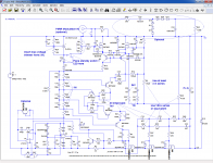
Here is the series schematic with some explanatory annotations:
Most should be clear enough and need no further explanation, here are the details for the rest:
About Q8:
It is reverse-connected in order to use its B-E junction as a 9~10V zener.
The zener is used to "park" the output of U1 in its linear range when the current regulation is inactive.
With most types of opamps, it will improve the response speed: an opamp is not designed as a comparator, and when used as such, it takes some time to return in linear mode when it has been saturated.
A transistor is used rather than a regular 9V zener, because the leakage of a zener is significant and would alter the current regulation threshold.
PSRR modulation:
The topology of this supply lends itself to these kind of tests.
The modulation input injects a signal into the output with a gain of ~2dB, between 20Hz and 20kHz (not ruler-flat, but acceptable).
Of course, depending on the output capacitance and current drawn, the slewrate might be insufficient to follow fast/high amplitude modulation.
Beware of the reference potential: to the positive GND. It could be necessary to use an insulation transformer to safely couple the signal.
The voltage doubler:
This only applies to the series version, and is a way of eliminating the no load problem discussed earlier.
The capacitive supply provides the ~0.5mA required to cancel the current injected by the sharing divider
Attachments
The no-load issue could also be addressed by buffering the divider:

Using a large power device for this task is ridiculous overkill, but no low-power transistor exist at this voltage level.
A BJT could also be used since SOA is not a concern here, but very high voltage BJT's tend to have a ridiculously low β for collector currents <1mA.
To conclude, an important reminder: all the examples and circuits presented in the previous posts are just educated extrapolations supported by sims: none has been built and tested in reality.
The bits and pieces composing them (shunt reg, etc) have been individually used and tested, but in other contexts.
The only complete circuit that has actually been built and tested is the base Elektria.
Needless to say that circuits do not always behave the way they are supposed to, so be prepared for some debugging work.
Attachments
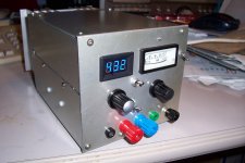
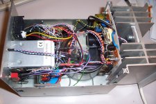
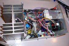
Elektria has now found a home: in the end, I built the case from scratch, to minimize the waste of space.
The dimensions are 23x11x13cm, which is satisfyingly compact for a linear supply capable of putting out 100 useful watts of DC power.
The dimensions are 23x11x13cm, which is satisfyingly compact for a linear supply capable of putting out 100 useful watts of DC power.
Attachments
The matter is in your own hands then: I sell nothing, I have no PCB design to offer, and anyway Elektria can be built for currents ranging from a few tens of mA to a few amps, and for voltages from 100V to several kV, with various possible references, current-control schemes, thus an universal PCB is impossible, or at least very unpractical.I want one.
If you want to simply copy my build, you can build it on perfboard, as I did, but I recommend you use a purely conventional 50Hz transformer, because the converter input requires a specific transformer and minimal precautions.
I built it around this transformer, because I had it available, but the chances you have such a transformer lying around are small, so the reasonable thing to do is to use a 380 to 420V, >250VA transformer
NMOS FETs can do >1300V without the need for cascoding, so no problem there (you can parallel them for higher power).
For the PNP drivers, reusing the same kind of resistor trick as I did is not possible for 1300V (not realistic anyway), so 3 to 5 cascode stages would be required, but that shouldn't be a problem, because MPSA92's are incredibly cheap, their quality doesn't matter (most of the semi's of my build are just cheap chinese copies), and the number of cascodes will not affect in any way the performances.
BTW, why limit yourself to 200V as a low limit? Going to zero costs nothing, and even if you think you won't need it 99% of the times, the 1% will come and bite you at some point in the future.
I will post a schematic adapted for voltages up to 1.5kV in the next few days.
Welcome to the Elektr⚡a club!
I too like using the known fake parts. Makes things more exciting with an air of danger.
All of your designs are very interesting.
Maybe put it all in book form?
Cheers
-
") I am going to think about building something compact for my bench based on your design.
I am going to think about building something compact for my bench based on your design.- Status
- This old topic is closed. If you want to reopen this topic, contact a moderator using the "Report Post" button.
- Home
- Amplifiers
- Power Supplies
- ELEKTR⚡A is a true High-Voltage lab supply, truly DIY-friendly