Test module design for TPS7A47 reg shows such capacitor too (C4 in fig. 6 on page 7).
Ah, I did not realize the post was about the 7A4701 variant. I would probably put a spot for it on the PCB but not populate it until you can verify startup and transient response is normal with it.
low noise LDO
I believe that you have the two feedback resistors swapped. The 10K should go to ground and the 110K to Vout.
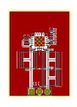
I also see that you still have a power ground connection from the Vin cap looping around to the top of the package. I can't see the Vout cap but I assume it is also returned to that skinny connection to the power pad. I recommend that those caps be placed so that their grounds are inline with the power ground pin coming in from the three pin connector. This will minimize the loop area. I have attached a schematic and top copper layout as I recommend. The only difference is that I've split the output cap into two 22uF/50V devices because it is a bit less expensive and easier to lay out. I also have not stitched the top and bottom ground planes together, but would do so.
I've been through 3 iterations of PCBs and almost $200 later and I still can't get the darn thing to work.

Can anyone spot my flaw? Other than the fact that the pin 1 dot is flipped the wrong way.
When I power it on it sits around 1.5v.
I believe that you have the two feedback resistors swapped. The 10K should go to ground and the 110K to Vout.
I also see that you still have a power ground connection from the Vin cap looping around to the top of the package. I can't see the Vout cap but I assume it is also returned to that skinny connection to the power pad. I recommend that those caps be placed so that their grounds are inline with the power ground pin coming in from the three pin connector. This will minimize the loop area. I have attached a schematic and top copper layout as I recommend. The only difference is that I've split the output cap into two 22uF/50V devices because it is a bit less expensive and easier to lay out. I also have not stitched the top and bottom ground planes together, but would do so.
Attachments
Haha, you're right I did have the resistors swapped. Workin' now ")
The two caps at the bottom where the "10u" text is are the in/out caps.
Where they meet is where the ground connection is and the ground connection leads up to the small trace you spoke of and into the ground origin point.
Is that not correct?
Also why do I see a difference in location for the input cap between these two pictures?


Which one should I choose and why?
The two caps at the bottom where the "10u" text is are the in/out caps.
Where they meet is where the ground connection is and the ground connection leads up to the small trace you spoke of and into the ground origin point.
Is that not correct?
Also why do I see a difference in location for the input cap between these two pictures?
Which one should I choose and why?
which one
As I recall you are bringing input, ground, and output all to what is equivalent to a 3 pin header. That matches the top layout. And by putting the input and output bypass caps down there you minimize the loop that current flows through from input through the input cap and to ground. Similarly for output through the output cap and to ground. The layout for the negative regulator, the bottom layout, has ground coming in from one side and the power connections from the other side. It takes advantage of the multiple no connects you have to allow a solid ground connection to the center pad. You don't have that same pinout advantage for the positive regulator. The top layout is the one I pretty much copied in the layout given in the earlier reply and it will work for both the positive and the negative regulator.
As I recall you are bringing input, ground, and output all to what is equivalent to a 3 pin header. That matches the top layout. And by putting the input and output bypass caps down there you minimize the loop that current flows through from input through the input cap and to ground. Similarly for output through the output cap and to ground. The layout for the negative regulator, the bottom layout, has ground coming in from one side and the power connections from the other side. It takes advantage of the multiple no connects you have to allow a solid ground connection to the center pad. You don't have that same pinout advantage for the positive regulator. The top layout is the one I pretty much copied in the layout given in the earlier reply and it will work for both the positive and the negative regulator.
addendum
The top connection ground for the noise reduction cap and the feedback resistor is a low current connection and is correct. The high current ground connection is made via the multiple no connect pins and is where the ground side of the 10uF input cap and the ground side of the output can should be placed.
The top connection ground for the noise reduction cap and the feedback resistor is a low current connection and is correct. The high current ground connection is made via the multiple no connect pins and is where the ground side of the 10uF input cap and the ground side of the output can should be placed.
- Status
- This old topic is closed. If you want to reopen this topic, contact a moderator using the "Report Post" button.
- Home
- Amplifiers
- Power Supplies
- TPS7A4701 and TPS7A33 PCBs?