
That's compensation, not a native solution by layout and parts choices, but its alright for your experimental 1.3 inspired & self made reg on the quick. You know, I never released the 1.2R for a GB because of its sensitive nature on such things and its use of expensive and widely faked NOS JFETs. I understand the test building and load matching difficulties for a higher spec shunt from experience. So it remained the favorite shunt reg of few skilled and basic lab equipped DIYers that took on the battle to successfully put it together. To make the 1.3 reliable to build and universally useful, when it has even more internal gain than the 1.2R while behaving itself also, wasn't an easy task at all...
Is the transformer secondary voltage chosen to suit the required dc voltage needed ?
The goal is to achieve rectified DC Vin at around 5V more than Vout. As it was for the 1.1 BiB. Rectified DC=(Vac*1.414)-1.4V diodes drop. I.e. 9Vac for 5-7V out, 12Vac for 8-10V Vout, 15Vac for 11-15Vout, 18 Vac for 16-19Vout and so on and so forth up to 33 Vac max not to burn some JFET.
It would strictly work for less Vdif. Because CCS mA sagging starts only at Vin-Vout <1.7V for ~200mA settings. At 600mA CCS it starts at Vin-Vout <2.5V. But we want more headroom for mains tolerances and better behavior of M1 for parasitic capacitance reasons. Thus 5V or some more is a good figure.
Checking to see if my calculation for R1 current limit resistor are correct.
I have an 18VAC transformer. So I am figuring about 24VDC out of my rectifier. The regulators will be set to +/- 15VDC output. Max current load is 5mA. If I use a 4.7 ohm resistor I calculate that the CC would be approximately 128mA. Does this sound correct?
I have an 18VAC transformer. So I am figuring about 24VDC out of my rectifier. The regulators will be set to +/- 15VDC output. Max current load is 5mA. If I use a 4.7 ohm resistor I calculate that the CC would be approximately 128mA. Does this sound correct?
Hi Salas is it possible to run a slightly higher output voltage, 45V with a low current demand of around 30ma
Dangerous for J1 & J3 as they will exceed their 40V spec in such an occasion. A modification that could work at your requested voltage area is to replace J1 & J3 and their source resistors with 22k resistors across drain pad to source resistor end pad and use a 36 Vac transfo. Also to remove Vrr so the trimmer can reach higher.
Yes or 1/4W even. There are 10mm distanced pads for them. Prefer 50ppm. No more than 100ppm anyway. I used Xicon 1/4W 50ppm and Beyschlag 0.4W 50ppm mainly. But whatever good that's stocked and it fits will do. For R9 buy 1kΩ alternative also. Its about when forced to use much spare current because some application changes states of consumption for instance. Not to oscillate in the transition because with say 0.5A spare burned in M2 its transconductance and temperature will go up and its characteristics will change. Most beta testers used 1K that I had designated for safety but they ended up using little spare current which is much better for M2's current noise and temperature (plus smaller sinks). Up to 200-250mA spare current R9 270R is fine and the impedance stays lower up at 1MHZ vs 1k. I don't know yet if there is a subjective benefit in that or to put 1k R9 and forget it. When some beta tester listens between those two gate stopper values where 270R is enough for stability and has a finding I will decide. Pay attention, spare current is what remains to be burned in M2 after load's draw. Not the M1 CCS limiter's R1 mA setting. Spare=CCS mA minus Load's draw mA.
Also for those wanting the reg for no higher than 20V output applications, C2 can be 25V type. And VR1 be 10k for more turns focused in the range of interest. Especially for digital because clocks are supposed to appreciate low 1/f noise C2=470uF/25V Nichicon KZ or 470uF/35V Nichicon ES BP are nice. C3 remains 33uF/50V ES BP or 33uF/50/100V KZ or 100uF/50V Pana FC.
What happens with higher value C2 is the 1/f (subsonic) noise lessens vs the 220uF median (470uF is magenta line when 220uF is red line in post#1 2nd chart) but the voltage rise to nominal is slower at start up until it fully charges with the little mA that are available for that. I don't mean minutes, I mean few seconds "soft start". Some may find lower value C2 caps liked better as "bit faster, more open" in some app or not, that's the user's business to evaluate. Its a low noise reg anyway with no filtering difference from 20Hz up with as low as 100uF C2 even. As that chart also shows. In general with any value C2 its a soft start reg. It does not "spike" to over-voltage at turn on. Its temperature induced output voltage drift to full warm up (1 to 1.5%) is going down also, not drifting up. In other words your digital chips, even if any is directly fed without a local reg in its pcb design, they are safe sir thank you")
Also for those wanting the reg for no higher than 20V output applications, C2 can be 25V type. And VR1 be 10k for more turns focused in the range of interest. Especially for digital because clocks are supposed to appreciate low 1/f noise C2=470uF/25V Nichicon KZ or 470uF/35V Nichicon ES BP are nice. C3 remains 33uF/50V ES BP or 33uF/50/100V KZ or 100uF/50V Pana FC.
What happens with higher value C2 is the 1/f (subsonic) noise lessens vs the 220uF median (470uF is magenta line when 220uF is red line in post#1 2nd chart) but the voltage rise to nominal is slower at start up until it fully charges with the little mA that are available for that. I don't mean minutes, I mean few seconds "soft start". Some may find lower value C2 caps liked better as "bit faster, more open" in some app or not, that's the user's business to evaluate. Its a low noise reg anyway with no filtering difference from 20Hz up with as low as 100uF C2 even. As that chart also shows. In general with any value C2 its a soft start reg. It does not "spike" to over-voltage at turn on. Its temperature induced output voltage drift to full warm up (1 to 1.5%) is going down also, not drifting up. In other words your digital chips, even if any is directly fed without a local reg in its pcb design, they are safe sir thank you
This probably be a stupid question.
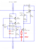
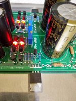
From your schematic for Neg rail, emiter of q1 is connected to negative side of c1 but in the picture of PCB I can see a trace running from -c1 to collector of q1.
Also an emitter of q1 is connected to r3 and r4. Should it be an opposite or am I missing something?
From your schematic for Neg rail, emiter of q1 is connected to negative side of c1 but in the picture of PCB I can see a trace running from -c1 to collector of q1.
Also an emitter of q1 is connected to r3 and r4. Should it be an opposite or am I missing something?
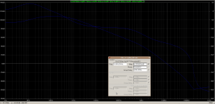
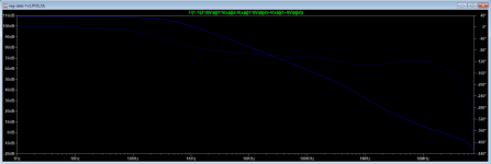
Schematic is intrinsically unstable in its initial version, see the OLG in the first attached file - the ULG is 13.5 MHz and the phase shift is -183 deg. No more words are needed.
Introducing the RC frequency compensation network proposed by @Selfy (R=100 Ohm, C=1nF) the OLG becomes as shown in the second picture - now the ULG is 2.3 MHz and the phase shift is 96.7 dB which is much, much better - the phase margin is more than 80 deg.
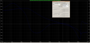
The only thing which scratch my eye is the big phase excursion in the region 1 kHz - 100 kHz.
The both simulations are performed with output capacitor 100 uF with ESR=0.1 Ohm as suggested in the initial document. BTW, finding such capacitors and relying on their constant ESR over time is not an easy task.
And combining with the fact that the capacitance added on the regulator's output via attached load is almost impossible to predict a-priory, the possibility of oscillation becomes bigger and bigger.
However, the other advantage of the proposed compensation network is that it permits on the regulator's output to be used bigger capacitors with more "normal" ESR of, let say 50-60 milliOhm.
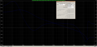
On the third picture you can see the OLG with attached capacitor 1000 uF, ESR=0.06 Ohm on the output. The nasty belly is compensated by 20 dB which is not bad, isn't it?
And on the fourth picture is plotted the schematic's output impedance - 38 uOhm on 1kHz. This proves that the insertion of the compensation network does not deteriorate the regulator's output impedance.
In conclusion - very good results for such a simple schematic.
Two shortcomings though - the poor phase linearity and the poor thermal stability of the output voltage.
Introducing the RC frequency compensation network proposed by @Selfy (R=100 Ohm, C=1nF) the OLG becomes as shown in the second picture - now the ULG is 2.3 MHz and the phase shift is 96.7 dB which is much, much better - the phase margin is more than 80 deg.
The only thing which scratch my eye is the big phase excursion in the region 1 kHz - 100 kHz.
The both simulations are performed with output capacitor 100 uF with ESR=0.1 Ohm as suggested in the initial document. BTW, finding such capacitors and relying on their constant ESR over time is not an easy task.
And combining with the fact that the capacitance added on the regulator's output via attached load is almost impossible to predict a-priory, the possibility of oscillation becomes bigger and bigger.
However, the other advantage of the proposed compensation network is that it permits on the regulator's output to be used bigger capacitors with more "normal" ESR of, let say 50-60 milliOhm.
On the third picture you can see the OLG with attached capacitor 1000 uF, ESR=0.06 Ohm on the output. The nasty belly is compensated by 20 dB which is not bad, isn't it?
And on the fourth picture is plotted the schematic's output impedance - 38 uOhm on 1kHz. This proves that the insertion of the compensation network does not deteriorate the regulator's output impedance.
In conclusion - very good results for such a simple schematic.
Two shortcomings though - the poor phase linearity and the poor thermal stability of the output voltage.
Attachments
This probably be a stupid question.
From your schematic for Neg rail, emiter of q1 is connected to negative side of c1 but in the picture of PCB I can see a trace running from -c1 to collector of q1.
Also an emitter of q1 is connected to r3 and r4. Should it be an opposite or am I missing something?
No you are not missing something. Crt missed something and I did not catch it. Q1's orientation print in the negative rail should have been reversed. Tricky, it works all the same in test for steady circa -0.6V across R1 following well with the positive section's R1 voltage. That is why the glitch passed unnoticed. The negative section's Q1 can be positioned the other way around than its now printed of course because the base pin is the middle one in those types. To be typical and have closer base current to Q1 positive.
I will put this corrected orientation down in the build guide and will see to reverse the solder mask print in the future pcb runs.
Thanks for noticing.
Attachments
Schematic is intrinsically unstable in its initial version, see the OLG in the first attached file - the ULG is 13.5 MHz and the phase shift is -183 deg. No more words are needed.
Introducing the RC frequency compensation network proposed by @Selfy (R=100 Ohm, C=1nF) the OLG becomes as shown in the second picture - now the ULG is 2.3 MHz and the phase shift is 96.7 dB which is much, much better - the phase margin is more than 80 deg.
The only thing which scratch my eye is the big phase excursion in the region 1 kHz - 100 kHz.
The both simulations are performed with output capacitor 100 uF with ESR=0.1 Ohm as suggested in the initial document. BTW, finding such capacitors and relying on their constant ESR over time is not an easy task.
And combining with the fact that the capacitance added on the regulator's output via attached load is almost impossible to predict a-priory, the possibility of oscillation becomes bigger and bigger.
However, the other advantage of the proposed compensation network is that it permits on the regulator's output to be used bigger capacitors with more "normal" ESR of, let say 50-60 milliOhm.
On the third picture you can see the OLG with attached capacitor 1000 uF, ESR=0.06 Ohm on the output. The nasty belly is compensated by 20 dB which is not bad, isn't it?
And on the fourth picture is plotted the schematic's output impedance - 38 uOhm on 1kHz. This proves that the insertion of the compensation network does not deteriorate the regulator's output impedance.
In conclusion - very good results for such a simple schematic.
Two shortcomings though - the poor phase linearity and the poor thermal stability of the output voltage.
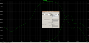
Are you talking about Selfy's initial and then the compensated?
Because the UltraBiB simulates like this for OLG:
Attachments
- Home
- Amplifiers
- Power Supplies
- Salas SSLV1.3 UltraBiB shunt regulator