Hi, I built a few of these power supplies a while ago. Looking now at the schematic I cannot remember why I chose to use an LM317 on both rails instead of going for an LM337 on the negative supply.
Is there a reason why this shouldn't work? - I've used this supply on a preamp that I'm fault finding and I just wanted to see whether I would be better off regulating the negative rail to eliminate potential problems with the PS.
Thanks,
Simon.
Is there a reason why this shouldn't work? - I've used this supply on a preamp that I'm fault finding and I just wanted to see whether I would be better off regulating the negative rail to eliminate potential problems with the PS.
Thanks,
Simon.
Attachments
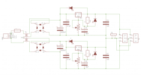
Conceptually and operationally I would say no.
You might have been forced to use an LM317/LM337 if your transformer had a fixed centre tapped secondary but since you have access to both secondaries separately I see no problems with your chosen solution.
Maybe you forgot that you had an AHA! moment.
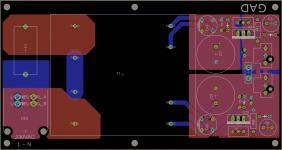
Of course it may be the case that, in audio terms, people will start to have kittens about ground... or something else. Me, not so much but perhaps you might revisit your PCB and check it. I cannot see the bottom layer and your top section appears to have a split plane?
You might have been forced to use an LM317/LM337 if your transformer had a fixed centre tapped secondary but since you have access to both secondaries separately I see no problems with your chosen solution.
Maybe you forgot that you had an AHA! moment.
Of course it may be the case that, in audio terms, people will start to have kittens about ground... or something else. Me, not so much but perhaps you might revisit your PCB and check it. I cannot see the bottom layer and your top section appears to have a split plane?
Last edited:
I cannot remember why I chose to use an LM317 on both rails instead of going
for an LM337 on the negative supply. Is there a reason why this shouldn't work?
This is fine, and the 317 is better than the 337.
Thanks guys, nice to have some confirmation. The split on the top plane is between unregulated and regulated positive supply.
Shows how bad my old eyes, reverse engineering skills, are.
Unrelated but just to be a pedant... Your primary side may violate regulatory requirements in respect of creepage/clearance Live to Neutral.
Something like this one here,
https://www.electricalsafetyfirst.org.uk/mediafile/100015224/Chargers.pdf
Page 3) Other,
Other:
The measured creepage distance between Live and Neutral before any fusing was 2.1mm and the measured clearance distance was 1.8mm, the minimum requirement is 2.4mm.
Yes, looks as though the clearance between the live pins of the molex connector and the neutral pour are well below that tolerance. I have a vague memory of checking the clearance limits but probably not against regulatory requirements... thanks for the link, I'll do a bit of Christmas reading  .
.
.I'll do a bit of Christmas reading
Whatever 'floats your boat'. In fact it looks like it is worth a read.
I was just looking for an example. Last time I did this stuff I ended up joining BSI so I could get the standards half price rather than relying on someone else's 'word of mouth'.
It looks like
Electrical Safety First - The UK's Electrical Safety Experts
might have submitted a bunch of chargers to BSI in Hemel Hempstead for appraisal. The pictures suggest that they are 'Pre-Loved'.
Otherwise, somehow, they still got sold in the UK.
It is one of the things that puts me off buying nondescript 'drop shop' stuff from Ebay, especially when it is mains operated. If it does not blow itself up it is likely to be a safety hazard.
your layout will not perform at the best that a 317 can achieve.
If I am reading your layout correctly then it appears that the top left pin of the VR is connected to the blue plane and the -ve end of C5 is also connected to the blue plane.
But these two connections are far apart.
The output Zero Volts is also on the blue plane.
These three tappings into the blue plane are supposed to all be at the same voltage.
But you have them spread about at distances that can't get much bigger.
The closer you can make these three tappings the better the regulation.
Aim to get VR pin1 + C5-ve +Zero Volts out, to be near coincident or within a couple of mm of each other.
Similarly the output resistance/impedance is affected by the length of the trace from reg OUT to Zero Volts out. Minimise this distance.
The negative has to follow the same laying out philosophy.
The VR -ve end +C8 -ve end and -ve out all need to be very close to each other.
and reg out needs to be very close to zero volts out.
Last edited:
If I am reading your layout correctly then it appears that the top left pin of the VR is connected to the blue plane and the -ve end of C5 is also connected to the blue plane.
The component U$1 is a pot (i forgot to set the right identifier in Eagle), IC1 is the regulator. Regulator input is the left red plane and output is to the right red plane.
Looking at the layout again in the light of your comments I can see that it could have been much tighter... I'll work further on the schematic before I get any more of these boards made up.
Thanks for the advice.
For what purpose is the PSU?
Hi, I'm using this one for a phono stage I'm working on (post 35 in this thread)
That's how I interpreted your layout.The component U$1 is a pot
Yes, that's what I could see.IC1 is the regulator.
Again,Regulator input is the left red plane and output is to the right red plane.
that's what I could see.
The schematic is correct. But it is simplified to the point it is misleading you into assuming that all traces that are connected together have the same voltage at all points on any part of a trace. Similarly on a plane the simplified schematic assumes all points on the plane are at the same voltage. That is not what occurs on the PCB.Looking at the layout again in the light of your comments I can see that it could have been much tighter... I'll work further on the schematic
You have to make the layout take account of these "hidden" voltage drops. The easy way is to make the important points that NEED the same voltage to be coincident on the PCB layout.before I get any more of these boards made up.
.......
That's why
should be rearranged to bring these three points/tappings together.VR pin1 + C5-ve +Zero Volts out,
Last edited:
Andrew, when you talk about the VR are you referring to the IC or the sum of the components that make up the regulator? I was a bit confused by your first post:
By the way, I like your comments as they force me to think about and try to understand what's going on in the circuit.
Should I take this to mean the grounded pin of the potentiometer?it appears that the top left pin of the VR is connected to the blue plane
By the way, I like your comments as they force me to think about and try to understand what's going on in the circuit.
I've got to admit, I don't really understand what the negative effects of the trimmers are.
AFAIK the track is a thick film material... cermet? It is not of itself 'low noise' performance. Electrical contact is by means of metal fingers...
M43P103KB40 | Vishay 43P Series 20-Turn Through Hole Trimmer Resistor with Pin Terminations, 10kΩ +-10% 1/2W +-100ppm/degC Side Adjust | Vishay
Contact Resistance Variation (Max.) 1% or 1Ω (whichever is greater)
Might not help but presumably for audio the major concern is how that might vary with vibration. If you are playing Thrash DubJazz with your regulator sat on top of the speakers then you might lose a bit of purity and end up with Thrash DubGrunge.
Use run-of-the-mill electrolytic capacitors for C4 and C7. Some brands of LM317 become unstable when the losses of the output capacitor are too small. I once connected an LM317 to two 10 uF X5R ceramic capacitors in parallel, which turned my LM317 into a sawtooth oscillator. The capacitors themselves worked as loudspeakers, so you could hear a beeping sound coming from the board. Connecting a 47 uF cheap aluminium electrolytic capacitor in parallel solved the problem.
- Status
- This old topic is closed. If you want to reopen this topic, contact a moderator using the "Report Post" button.
- Home
- Amplifiers
- Power Supplies
- Is there anything wrong with this PS design?