YH11068A Schematic update
(I've joined the forum primarily to post this)
trobbins: I saw a post of yours more recently than this thread, saying that you've not completed the schematic. Is that still the case?
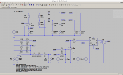
I've created a schematic in LTSpice from your hand drawn notes, but there are probably some errors... In particular, I've defined a node "Vx" as the power supply to the opamp, but I'm not clear on how it is supplied.
Anyway, does this look right to you? (wiring only - part designators, values, and other static are all up in the air ATM)
It would be nice to actually get this simulating in LTSpice (hoping that the LT1243 is very similar to the UC3843A).
It would also be nice to hack it with an opto in the feedback line so that the outputs are isolated/floating.
Any corrections would be appreciated.
(I won't bother posting the actual .asc file until it's closer to being correct)
(I've joined the forum primarily to post this)
trobbins: I saw a post of yours more recently than this thread, saying that you've not completed the schematic. Is that still the case?
I've created a schematic in LTSpice from your hand drawn notes, but there are probably some errors... In particular, I've defined a node "Vx" as the power supply to the opamp, but I'm not clear on how it is supplied.
Anyway, does this look right to you? (wiring only - part designators, values, and other static are all up in the air ATM)
It would be nice to actually get this simulating in LTSpice (hoping that the LT1243 is very similar to the UC3843A).
It would also be nice to hack it with an opto in the feedback line so that the outputs are isolated/floating.
Any corrections would be appreciated.
(I won't bother posting the actual .asc file until it's closer to being correct)
An externally hosted image should be here but it was not working when we last tested it.
Hi, your schematic is not linking properly. No I haven't attempted to redraw my hand-drawn schematic, so any re-draw would be a help, given that if sections of the schematic do not make sense (given what is known with normal use of those IC's) then I'll get the pcb out and confirm where the actual traces go.
Oops, I hadn't completed the upload to Imgur. I think this works:-
YK110068A boost converter - prliminary schematic - Imgur
(The FAQ here was no help, it mentions links to albums etc. in user control panel that aren't there)
YK110068A boost converter - prliminary schematic - Imgur
(The FAQ here was no help, it mentions links to albums etc. in user control panel that aren't there)

Given it is a Single Switch Flyback Converter the control IC is likely to be a UC3845, limited to 50% duty cycle. As such slope compensation is supposedly not needed. It would be for continuous inductor current when operated above 50% duty cycle. As I suggest that does not apply here.
Looking at the circuits that have been developed, reverse engineered, so far the inclusion of the LM358 appears to be an afterthought because someone got the compensation, and possibly something else, wrong. If you wish to go 'hard core' then...
Seegons Flyback Converter
Unfortunately it seems you are trying to reverse engineer something designed by someone who does not know much, copy catted by numerous others, that may well be the worse solution to your problem.
Simple case is that both input and output currents will be discontinuous, nominally square waves. The input supply gets hammered, huge square waves, and output ripple is horrible so, being you, you will start asking how much extra filtering you can add.. lipstick on a pig.
Given you are trying to reverse engineer a piece of dirt I assume that end game is you want to lay out your own PCBs and... Elsewhere I have suggested that a current fed push-pull might be a better solution.
Power supply options for tube preamp
Would you wish to collaborate on my 'Road to Fail'?
Your negative comments on these devices may well be correct and justified, certainly the ripple you mentioned is evident.
But I prefer to get the schematic correct first, before passing judgement.
I do find the presumptive tone of your response curious:-
The only problem I have mentioned is the lack of a complete schematic to this device
Yet from nothing more than that, you have somehow determined my nature and motivations?
In fact, your presumptions have gone right of the rails here. I most certainly do not want to recreate this device in another form.
(To build a switching HV supply from scratch, I would do much more research into possible solutions, including what you have suggested.)
My aim here is completely the opposite - These things are dirt cheap and already made.
I want to investigate their potential as a cheap and cheerful, ready made, source of HV. To be used as is, or with only minor modification.
To do that properly, a schematic is needed.
For the applications I have in mind, some pig lipstick may well be sufficient...
(Nixie tubes, Geiger counter, Electrophoresis, Testing of insulation, MOVs etc)
But I prefer to get the schematic correct first, before passing judgement.
I do find the presumptive tone of your response curious:-
...may well be the worse solution to your problem.
The only problem I have mentioned is the lack of a complete schematic to this device
Not even sure what that is supposed to mean. I've just joined this forum, and asked a simple question.... so, being you, you will start...
Yet from nothing more than that, you have somehow determined my nature and motivations?
Why would a bad design become an inspiration to reproduce it?Given you are trying to reverse engineer a piece of dirt, I assume that end game is you want to lay out your own PCBs
In fact, your presumptions have gone right of the rails here. I most certainly do not want to recreate this device in another form.
(To build a switching HV supply from scratch, I would do much more research into possible solutions, including what you have suggested.)
My aim here is completely the opposite - These things are dirt cheap and already made.
I want to investigate their potential as a cheap and cheerful, ready made, source of HV. To be used as is, or with only minor modification.
To do that properly, a schematic is needed.
For the applications I have in mind, some pig lipstick may well be sufficient...
(Nixie tubes, Geiger counter, Electrophoresis, Testing of insulation, MOVs etc)
Well said intabits - some posters seem to insert unneeded diatribe into a thread.
With respect to your draft schematic (I appreciate LTSpice may not have applicable parts, but I'll list items for completeness):
- The linear reg is a 78L09, with an output filter cap.
- output rectifier configuration is half-wave
- opamp V+ pin 8 connects to +9V supply (I missed a via link). C3 appears to be a local bypass to the opamp package.
- opamp output pin 1 has a 15k pull up to the +9V supply.
- opamp pin 6 pull up to +9V is 15k (not 8k), and 15k to pin 2 (not 8k).
I've enjoyed buying in a few of this style of dc/dc over the years to see how convenient they are for valve amps, and in general I've found their pcb layouts to be pretty good considering the simple double-side format. As such, they manage switchmode transient current loops pretty well, and I'm hard-pressed to identify ways to assist noise mitigation below what I reckon is insignificant anyway in a valve amp. Only sometimes can I identify the simple of addition of an smt cap to further minimise loop area.
So for me it is more about defining how they manage themselves for uvlo and ovlo, startup and output overloading.
As far as I need to be concerned you have resurrected a Zombie thread with a Wish List.
Here you go.. Broken Thing.
Next thing you will be asking how to design the magnetics and compensate the loop properly. Perhaps you should learn how to speak non pretentious Australian first.
...
I guess that hack would work if you knew some stuff but it is probably best to float the idea and get someone else to work it out for you... because you are not going to hack an opto on that board.It would be nice to actually get this simulating in LTSpice (hoping that the LT1243 is very similar to the UC3843A).
It would also be nice to hack it with an opto in the feedback line so that the outputs are isolated/floating. Any corrections would be appreciated.
DC-DC Boost Converter 8-32V 12V to +-45V-390V High Voltage ZVS Board Module NEW | eBayFor the applications I have in mind, some pig lipstick may well be sufficient...(Nixie tubes, Geiger counter, Electrophoresis, Testing of insulation, MOVs etc)
So... nothing to do with, being on topic, Audio and/or Valves.This booster module has voltage stabilizing function. It is used for capacitance charging, hunting and deratization or as power supply of electromagnetic gun, electronic equipment, or test power supply of voltage or glow tube.
Here you go.. Broken Thing.
Next thing you will be asking how to design the magnetics and compensate the loop properly. Perhaps you should learn how to speak non pretentious Australian first.
...
Attachments
Every forum has at least one, and I flushed this one out with my very first post! Geez, I'm good!
trobbins:-
Thanks, I'll update the schematic with your corrections.
Except on the output, my schematic is correct there.
These modules often come with -ve outputs as well, ie: dual half wave.
(which is why isolation would be good - can get 800V)
The MF:-
Zombie thread?
Yes, but this was the best/only place to make my inquiry.
There's nothing wrong with resurrecting an old thread if you have new input, to wit: my schematic.
On topic?
Audio? - No.
Valves? - Slightly.
Directing a question to the original poster about a document provided in the very first post of the thread that he started? - 100%
get someone else to do work for me?
Only for checking the schematic.
My request for corrections was for this alone, not for the hacks and simulation I mentioned.
But if someone wants to, that would be great...
The link you posted?
Was that supposed to be an alternative power supply for the applications I mentioned?
('coz it's precisely the thing this thread is about)
Your third quote?
Huh? By whom, from where?
"If I knew some stuff", "Broken thing", "speak non pretentious Australian"?
These appear to be an attempt at some sort of put-downs or insults, but they actually reveal more about you...
"Next thing you will be asking..."
And the presumptions continue...
I've already spent more effort replying to your deranged last post that it deserved, but i did because it has been quite enjoyable.
"wish list"?
This originally had only one entry, but I've added a second:-
1/ For trobbins to check my schematic
2/ For you to pull your head in
Dear trobbins, in case you have not seen this, there is a easy and tested DIY solution in the forum already.
DIY Off-Line SMPS 300V @ 100ma experiment
Regards,
DIY Off-Line SMPS 300V @ 100ma experiment
Regards,
Tim,
I've updated the schematic:-
* Where you had no value, I've made a guess (2K7,10nf,100nF)
* The diodes have no part numbers (except the LED)
* I don't see a C3 on your drawing, I assume you mean what I've designated as C4
The attached ZIP contains the .ASY files for the parts that are not supplied with LTSpice. Dropping the lot into a single folder, and opening the .ASC should work...
This is all just for the schematic, no attempt has been made to get simulation working. I may play with that, but it would probably be a waste of effort.
http://www.diyaudio.com/forums/attachment.php?attachmentid=669643&stc=1&d=1521467691
http://www.diyaudio.com/forums/attachment.php?attachmentid=669646&stc=1&d=1521467691
(Still trying to work this forum out. FAQ says "click the arrow next to the 'Attachment Icon' ", but nothing happens. So I've just added the links above)
Hello all!
Thank you for circuit diagram and very clear picture of PCB YH11068A.
And I would like to present new corrected circuit diagram. Differs in partnumbering and some connections:
http://impulsite.narod.ru/power/dcdc/yh11068a/yh11068a_katafei777-001.jpg
http://impulsite.narod.ru/power/dcdc/yh11068a/yh11068a_boost_converter-v1.png
An externally hosted image should be here but it was not working when we last tested it.
An externally hosted image should be here but it was not working when we last tested it.
If there are pull-up resistors like R12, R13, then operational amplifier LM358 can be easy replaced by comparator LM393. IMHO.My power supply, unlike the schematics, does not use LM358 but instead LM393.
Last edited:
- Status
- This old topic is closed. If you want to reopen this topic, contact a moderator using the "Report Post" button.
- Home
- Amplifiers
- Power Supplies
- YH11068A 10-32V to 45-390V dc/dc - guess the control ICs