I suspect the M4-ATX design is using LTC3789 - High Efficiency, Synchronous, 4-Switch Buck-Boost Controller - Linear Technology for the 12v buck-boost. data sheet claimed eff is >90% better than I imagined mostly better cuz of synchronous rectification all tho some users report a lot heat. Like you say logic level power MOSFET's required. not sure what is driving the Io max of 20A (probably sensing device levels with accurate low value resistors / and eff goals.)
seems worthwile to look at their newer device/ apps here LT8705
I reckon you could probably get to 400W with TO-220 packages on real heat sinks. and allowing for a little lower eff. look at their eval. boards.
seems worthwile to look at their newer device/ apps here LT8705
I reckon you could probably get to 400W with TO-220 packages on real heat sinks. and allowing for a little lower eff. look at their eval. boards.
I would love to use those LTC3789/Modern chips driving some MOSFETS, however, because of the package they are in, they are not too DIY friendly, although I will consider them for a new design on a daughterboard, or to upgrade other projects.
I'm going to try BUCK/BOOST
I have an inductor I made using 17 TURNS, 30 parallel strands of #24 wire for a homemade super litz made from a degauss coil, would on a huge BLUE MS-184026-2 Arnold Toroid, so I believe it's equal to a #6AWG wire, so the Inductor is well within spec for this project.
http://powermagnetics.co.uk/pace-co...ores/super-mss-sendust-type-cores/ms-184026-2
I'm considering using a 150khz dual TL494 Master/Slave controller setup on a daughterboard (so I can change/upgrade it later), using the Master 494chip running from 24V, driving the Buck section Mosfet, and having the slave 494chip driving the boost section Mosfet.
I plan on having their feedback networks similar, with maybe a 0.05 or 0.1V difference between the two chips, so the buck chip is at full pulse width when the voltage is low before the boost chip comes on.
Being there is not much difference from 14.4 - 12V, most power running through buck-MOSFET, I doubt my efficiency would not be too bad on the buck even with a schottky kick-back diode............BUT
My Concern with power handling would be the
series Diode on the BOOST, however, I do have a HUGE heatsink, so I imagine two 4045s or three 3045s in parallel would handle the current.
I wonder, if you can use the push-pull option of a TL494 to run MOSFETS as synch rectifiers in buck/boost, I've been looking at it........
Last edited:
unless yer FLA batteries are nearby the PC , the wire sizes will need to be huge to a power a 500W DC/DC at 12V and not drop close to 10% eff. just on I^2*R losses.
500W at 12V = 40Amps
using 8 AWG wire from 2 rooms away loses about 2.5 V round trip giving copper loss ~100 Watts on top of yer buck-boost design. I didnt include imperfect connector losses > check here http://www.rapidtables.com/calc/wire/voltage-drop-calculator.htm
BTW Most of those cheapy inverters are easily getting 90+% eff around half power anyways.
EDIT It seems silly to establish a new design based on just a few parts on hand., you could probably get them for free samples. Heck they might give away a populated demo PCB you could hack, if you ask the right distributors rep nicely.
Last edited:
I'm aiming for 400-500 W too. 100V inputs with a 30-40A charger output.
I found a pretty good app note for Buck-boost design http://www.onsemi.com/pub_link/Collateral/AND8490-D.PDF
yours certainly would be simplified down in functionality, since yer not seeing a high input range and 3 stage battery charger. I would pay attention to the high side driver and debug that 1st (maybe just use a IR part). I need to add some kind a visual status display though.
I'm now in process of building the converter. I know it has been a while since I updated the thread - looking for work, change of living situation, etc, makes it a bit hard to be designing power supplies...............but now its being built.,
Main Outputs will be 12V, 5V, 3.3V with also an AUX 25V, (-12V) section, 5V Standby (5VSB), and also may add an amplifier IC to it for some speakers, just for if I need it when powering a computer.
Mosfets for both High-Side buck, and also Boost Mosfets, are HRF3205 x 4 paralleled.
My Return Diodes are 4X Paralleled MBR3040PT for the Buck section and 4X Parallelled STPS30L40CW (low Vdrop) for the Boost Section/Output
diode. (400A MOSFETS, 120A DIODES)
The 5V Buck Section uses 2X IRF3205 MOSFETS, and 2X Paralleled STPS4045CW Diodes. (200A MOSFETS, 80A DIODES)
The 3.3V Section uses 1X HRF3205 and 1X 60L40 Diode (100A MOSFET, 60A DIODE)
So this circuit should be pretty stout. I have mounted everything to the heatsink, and I am wiring up all the high-current paths, then I will proceed to build the controller using 2X sync'd TL494 for the buck/boost 12V section and Also 34063 and TL494 chips for the other voltages and parts of the circuit, hope to update you folks soon in the near future.
Last edited:
The 12V section of the Buck/Boost converter will have a traditional buck/boost schematic, like in the image I linked to, (post for a visual) but once again, I use 4X paralleled MOSFETS and 4X Paralleled Schottky Diodes in place of the singles on the schematic.
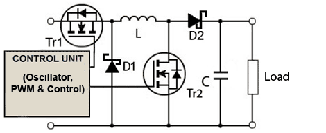
I will have twin TL494 chips, pulse-synched so they will pulse at the same time, for when it goes into boost mode, so both MOSFETS pulse at the same time. One chip (MASTER chip) will run the 12V buck, (SLAVE chip) will run the boost.
After much thinking about it, I still will use a power supply that is higher than the 12V battery supply rail, instead of having to worry about duty-cycle and charging of booststrap capacitors. I feel a regulated AUX 25 or 26V boosted rail to run my controller circuitry will give me the ease of driving my high-side MOSFETS gates with at least 10V when the battery is at 14.4V, but will also give them at least 15V gate drive when the battery sags, which will lower RDS-ON since they will be needing to drive more current anyway when the volts are low.
I know MOSFETS have a max drive of 20 Vgate, but I doubt that would be an issue with floating source terminals, and I can have the circuitry shut off if the battery sags to less than 7V if I'm concerned. I may think of using Gate Zeners, but I'm not sure they are even necessary, because I like the idea of the MOSFETS getting more gate drive the more the 12V battery rail sags below the boosted 25V+ AUX Rail.
All my buck sections, 12V, 5V, and 3.3V will drive the the High-Side MOSFETS from the 25V+ rail.
Any concerns, or comments about my MOSFET driving scheme, and any other concerns, greatly appreciated.
Last edited:
big batteries don't sag to 7V? and still support 4-500W power supplies, pretty much dead at 10V , why go through all this, aux. supplies etc.
use FETS like these ` 75cents apiece.
thought about the high side driver? should be worked out, can effect timing mismatch to lower side.
use FETS like these ` 75cents apiece.
thought about the high side driver? should be worked out, can effect timing mismatch to lower side.
big batteries don't sag to 7V? and still support 4-500W power supplies, pretty much dead at 10V , why go through all this, aux. supplies etc.
use FETS like these ` 75cents apiece.
thought about the high side driver? should be worked out, can effect timing mismatch to lower side.
Thanks for the Link for the Logic-Level MOSFETS, those would become handy in many projects.
 Thanks for your input as well.
BTW, Most all of your commercial 12V computer converters, advertise operation as low as 6-8V.
Big Batteries normally shouldn't sag that low, however, if you are starting a car in parallel with these batteries, or have any other large load in the system, there could be a transient voltage dip that the capacitors may not handle, so it's just planning for worst-case scenario to avoid a computer restart.
Actually I don't want the batteries to go below 11V, but I am planning on having adequate drive for the MOSFETS just in case.
For Example, I built a small 19.5V boost converter for my laptop bag powered with a 12V 4.5AH AGM battery using a 34063 PWM driver chip, feeding an NPN/PNP totem pole to drive a STP55NF06 MOSFET and discovered that the Boost converter loses it's ability to hold 19.5V when the battery sags to <8V Probably because of the Voltage drop of the Chip output stage +Totem Pole NPN, that it just doesn't have enough gate drive at that point to saturate the MOSFET. Yes, that battery is nearly depleted at that point, however, this is a low power device in comparison, not enough power to worry about blown MOSFETS, but makes a good example.
thought about the high side driver? should be worked out, can effect timing mismatch to lower side.
I will drive all my High-Side MOSFETS with NPN/PNP Totem Pole Configuration for reliability, The TL494 chips and totem poles driving the High-Side Mosfets for the Buck sections will be powered above the 12V Battery Rail with the AUX 25V Output. A 34063 Chip/IRF 630/MBR1620/small toroid inductor combination can easily generate this rail with little complexity. I can also run a 7815+NPN Buffer off the AUX 25V rail to power the TL494/Totem Pole Low-Side Driver for the Boost MOSFET. To turn on/off the Whole Power Supply, I can just turn on or off the AUX rail, which would power up the main PWM TL494 chips. I will have soft-start on all outputs.
Having the 12V section TL494s Synched Master/Slave is how my timing should be good, running the two chips combined as one controller in a sense. (I won't have the boost turn on when the buck is off for example, because the oscillators will be tied together with the CT terminal [see datasheet on sync'ing TL494's]). They will operate single-ended (push-pull disabled) and plan on 150-200khz since my BOOST inductor is low-perm Sendust Core.
keeping a 500W supply live while cranking a starter seems plain silly and counterproductive esp on a low batt condition with a huge load like that. I would just lockout anything lower than 10V and try supporting higher than 16V w/o damage, more likely to happen in my experience. You will always get some yahoo taking out a battery while the alternator is spinning. Look at inverter specs in these cases.
In fact a dual battery setup would be my 1st advise otherwise youll easily put the vehicle at risk w/o it. 500 W and a single 2-3 year old starter battery will need a tow truck in half an hour. I guess I don't understand your goal. yer gonna design and build this without ordering any parts? that seems like madness to my sensibilities. modern parts minimizing BOM would make it more effective and simple.
In fact a dual battery setup would be my 1st advise otherwise youll easily put the vehicle at risk w/o it. 500 W and a single 2-3 year old starter battery will need a tow truck in half an hour. I guess I don't understand your goal. yer gonna design and build this without ordering any parts? that seems like madness to my sensibilities. modern parts minimizing BOM would make it more effective and simple.
I don't need to order parts. I already have 9 HRF3205 and 2 IRF3205 (100A) MOSFETS all pulled from UPS.
I have LOTS of MOSFETS and schottky diodes of same part numbers, obviously if I am running parallels.
I plan on ordering some AUIRFP4004 MOSFETS (AUIRFP4004 International Rectifier | Mouser) (350A,40V)
in the near future for some projects, and I could always upgrade from parallel 4X HRF3205 to just 2X AUIRFP4004 simply by desoldering and replacing the MOSFETS, and retightening my steel clamp on the heatsink.
That's why I love DIY, upgrades are easy.
- Status
- This old topic is closed. If you want to reopen this topic, contact a moderator using the "Report Post" button.
- Home
- Amplifiers
- Power Supplies
- 12V TO 12V SMPS circuit topology choices