farnell  there is 5 things that i needed to order 10 of, the problem with getting anything from outside EU is that i need to pay a 8$ fea and tax on it, so if i just buy something super cheap or if someone sends me something for 50 cents i still ned to pay 8$, it is realy stupid
well i guess i will put in the order and i will just hope that it works
there is 5 things that i needed to order 10 of, the problem with getting anything from outside EU is that i need to pay a 8$ fea and tax on it, so if i just buy something super cheap or if someone sends me something for 50 cents i still ned to pay 8$, it is realy stupid well i guess i will put in the order and i will just hope that it works
Build questions
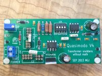
Thanks to j_thomas, i got a board and parts kit. Soldered last weekend, and just tried to power it up with a 9v battery... at first the LED was lighting up, but very dimly...barely lighting compared to photos on this thread.
So I tried some basic continuity tests and briefly touching the battery leads closer to the LED - (Pos to the square LED hole (near VR1) , and Neg to R1 (812r - actual) no dice... BUT, if i bypass R1 or connect the negative lead to the round LED hole (closer to Conn 2) then the LED lights up BRIGHTLY!!!
I also confirmed with my continuity tester that there is a path from the neg LED to Gnd, but I can't find the path from +Vin to the pos LED lead (hmmm?)
Finally - if I touch some of the legs from either transistor to with the Pos battery, and the Neg to the LED - leg, the LED lights up (various brightnesses depending on which leg).
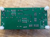
I was careful handling the transistors and diodes (no static). The LMC555 socket is has a chip labeled TLC555cp and the MCP1407 socket has a TC4420. I did not check diode values, but I just got a diode tester, and will follow up with those values... just wanted to get the basic question out here.
Im a generally handy person, but my soldering skills and theoretical electronics knowledge are beginner level. I did clean possible flux residue trackside with alcohol and a toothbrush several times, and also used a flashlight and magnifying glass to check I had not bridged any through-holes. (at my age, bare eyes don't do the job)
Anyone willing to help me debug the board or parts I may have botched?
Thanks! - Sixto.
Thanks to j_thomas, i got a board and parts kit. Soldered last weekend, and just tried to power it up with a 9v battery... at first the LED was lighting up, but very dimly...barely lighting compared to photos on this thread.
So I tried some basic continuity tests and briefly touching the battery leads closer to the LED - (Pos to the square LED hole (near VR1) , and Neg to R1 (812r - actual) no dice... BUT, if i bypass R1 or connect the negative lead to the round LED hole (closer to Conn 2) then the LED lights up BRIGHTLY!!!
I also confirmed with my continuity tester that there is a path from the neg LED to Gnd, but I can't find the path from +Vin to the pos LED lead (hmmm?)
Finally - if I touch some of the legs from either transistor to with the Pos battery, and the Neg to the LED - leg, the LED lights up (various brightnesses depending on which leg).
I was careful handling the transistors and diodes (no static). The LMC555 socket is has a chip labeled TLC555cp and the MCP1407 socket has a TC4420. I did not check diode values, but I just got a diode tester, and will follow up with those values... just wanted to get the basic question out here.
Im a generally handy person, but my soldering skills and theoretical electronics knowledge are beginner level. I did clean possible flux residue trackside with alcohol and a toothbrush several times, and also used a flashlight and magnifying glass to check I had not bridged any through-holes. (at my age, bare eyes don't do the job)
Anyone willing to help me debug the board or parts I may have botched?
Thanks! - Sixto.
Attachments
Hi, I find that you have placed wrong position of the U1 & U2.
The pin 1 of IC have dot mark on it and the silkscreen of pin 1 is square.
Please remove U1 & U2 and replace the new one.
Hope can help you
The pin 1 of IC have dot mark on it and the silkscreen of pin 1 is square.
Please remove U1 & U2 and replace the new one.
Hope can help you
Thanks to j_thomas, i got a board and parts kit. Soldered last weekend, and just tried to power it up with a 9v battery... at first the LED was lighting up, but very dimly...barely lighting compared to photos on this thread.
So I tried some basic continuity tests and briefly touching the battery leads closer to the LED - (Pos to the square LED hole (near VR1) , and Neg to R1 (812r - actual) no dice... BUT, if i bypass R1 or connect the negative lead to the round LED hole (closer to Conn 2) then the LED lights up BRIGHTLY!!!
I also confirmed with my continuity tester that there is a path from the neg LED to Gnd, but I can't find the path from +Vin to the pos LED lead (hmmm?)
Finally - if I touch some of the legs from either transistor to with the Pos battery, and the Neg to the LED - leg, the LED lights up (various brightnesses depending on which leg).
I was careful handling the transistors and diodes (no static). The LMC555 socket is has a chip labeled TLC555cp and the MCP1407 socket has a TC4420. I did not check diode values, but I just got a diode tester, and will follow up with those values... just wanted to get the basic question out here.
Im a generally handy person, but my soldering skills and theoretical electronics knowledge are beginner level. I did clean possible flux residue trackside with alcohol and a toothbrush several times, and also used a flashlight and magnifying glass to check I had not bridged any through-holes. (at my age, bare eyes don't do the job)
Anyone willing to help me debug the board or parts I may have botched?
Thanks! - Sixto.
You are correct, I looked closer and I have them both turned 180 degrees... Silly me, I thought the text printed on the chips should align with the text on the PCB.... Rookie mistake - I won't make it again... now to wait for the Haako desoldering iron to arrive...
On closer exam... did I also install the DIP switch backwards? it looks that way according to post 106... Hmmm that's 3 strikes!
Is there a chance I may be able to salvage the chips, or should I just order replacements?... nah, I probably am nowhere good enough to remove them without damage. New chips.... ah the joys of learning the hard way.
Thanks schmike!
Hi, I find that you have placed wrong position of the U1 & U2.
The pin 1 of IC have dot mark on it and the silkscreen of pin 1 is square.
Please remove U1 & U2 and replace the new one.
Hope can help you
Last edited:
I made exactly the same mistake with a new and upgraded processor chip for my Quad FM4 tuner. Quad supplied it on a little board, because it had a different pin layout. I shoved into the socket in with the chip ident aligned in the same way as the old chip. Wrong. Looking at the instruction, it needed to be installed the other way round - so the chip ident 180 degrees out.
Fortunately the device survived the trauma.
Craig
Fortunately the device survived the trauma.
Craig
When those Gerber files were created and posted, in October 2013, (seven years ago!), I felt there were two PCB fabs who were the cheapest and easiest for DIY builders to use:
At that time, those two fabs required different three-letter file extensions for the various Gerber files within the .zip archive. For example, the board perimeter ("edge cuts") layer needs to be filetype ".GML" for seeed , while it needs to be type ".GKO" for OSH Park. The layer describing drill holes needs to be file type ".TXT" for seeed, and file type ".XLN" for OSH Park.
Seven years ago, I thought it was equally likely that a Quasimodo builder would choose one or the other of these two fabs, so I provided two sets of Gerbers, one compatible with OSH Park and the other compatible with seeed. Every byte of the Gerber files is identical, the only differences are in the file type extensions. But that's what those two fabs required, to successfully build boards in October 2013.
Time has passed and the hobbyist / "maker" / DIY scene has exploded. There are now more than twenty PCB fabs for DIY builders to choose from. The wonderful and excellent website PCBShopper – A Price Comparison Site for Printed Circuit Boards will give you a price quote estimate from many of them, I strongly recommend you use it every time you order boards. It will tell you who is fastest and cheapest TODAY, including special promotional deals and 50% off sales.
In the subsequent seven years, after October 2013, it appears that just about 100% of the PCB fabs in Asia, have chosen to standardize upon the Gerber file naming convention used by seeed. In particular, the three Asian PCB fabs that I myself use most often (JLCPCB, Elecrow, PCBway), all accept seeed style Gerber files. So those are the ones you should send when you order Quasimodo boards, either surface mount (V3) or thru hole (V4).
I just had some boards made from PCB Prototype & PCB Fabrication Manufacturer - JLCPCB and was very happy with the price and delivery times. Much cheaper than OSH Park if you don't need the gold plating.

First off, Thank you Mark for the board and help in picking an oscilloscope (months ago).
Here is a shot of my competed board,

Transformer,

Shorted, as I understand how it should be shorted for 110v parallel primaries,

One secondary connected, I will be using two bridges on Prasi's compact PSU,

Here is the initial ring (scope was "zero'ed" as per manual)

After adjusting resistor,

Removed and read resistor,

The other secondary with same resistor setting,

Does this look like I have done everything correctly?
(I am a 52 year old woodworking machinery sales professional with no foundation in electronics or math, my hobby for 35 years has been woodworking, which wandered into speaker building and now amps for those speakers, so be nice if I have this all wrong... )
Thank you,
David.
Here is a shot of my competed board,
Transformer,
Shorted, as I understand how it should be shorted for 110v parallel primaries,
One secondary connected, I will be using two bridges on Prasi's compact PSU,
Here is the initial ring (scope was "zero'ed" as per manual)
After adjusting resistor,
Removed and read resistor,
The other secondary with same resistor setting,
Does this look like I have done everything correctly?
(I am a 52 year old woodworking machinery sales professional with no foundation in electronics or math, my hobby for 35 years has been woodworking, which wandered into speaker building and now amps for those speakers, so be nice if I have this all wrong...
)Thank you,
David.
Yep, I'd say you nailed it DaveFred! Fine-looking work, and great pics of it, too.
A couple little tips, though. Likely won't make more than a nibble of difference, but might on a different transformer.
Each primary winding can be shorted with its own jumper. That avoids the possibility that one winding will have a one-jumper short, while the other has three jumpers in series shorting it.
A carefully-built dual-secondary transformer MAY have similar-enough secondaries to use the same damping values on each, but there's no guarantee. Since QuasiModo only takes a few minutes (usually) to dial-in, might as well find the optimum value for each -- even though it may very well come out to about the same value.
You've now successfully damped each secondary -- congrats well done! But big transformers usually look into big rectifiers, which often have higher capacitance. Plus, not all rectifiers are created equal. I would consider reserving a little space near each bridge, and plan a final assessment for when the build is farther along. That way you'll be compensating the actual operating environment.
Still, this is great work, just as it is !
Cheers
A couple little tips, though. Likely won't make more than a nibble of difference, but might on a different transformer.
Each primary winding can be shorted with its own jumper. That avoids the possibility that one winding will have a one-jumper short, while the other has three jumpers in series shorting it.
A carefully-built dual-secondary transformer MAY have similar-enough secondaries to use the same damping values on each, but there's no guarantee. Since QuasiModo only takes a few minutes (usually) to dial-in, might as well find the optimum value for each -- even though it may very well come out to about the same value.
You've now successfully damped each secondary -- congrats
well done! But big transformers usually look into big rectifiers, which often have higher capacitance. Plus, not all rectifiers are created equal. I would consider reserving a little space near each bridge, and plan a final assessment for when the build is farther along. That way you'll be compensating the actual operating environment.Still, this is great work, just as it is !
Cheers
Last edited:
Yep, I'd say you nailed it DaveFred
A couple little tips, though. Likely won't make more than a nibble of difference, but might on a different transformer.
Each primary winding can be shorted with its own jumper. That avoids the possibility that one winding will have a one-jumper short, while the other has three jumpers in series shorting it.
I wasn't sure just how they were to be shorted.
Short each primary individually, or attach all the primary leads together.
Can someone clarify?
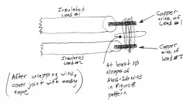
Short-circuit each of the other windings without increasing their wirelength at all. Not even 1 millimeter. I find it easy to do them one winding (one pair of wires) at a time, as diagrammed below. But any other scheme that doesn't increase wirelength at all, would be equally good.
After you do this a couple times, you'll learn to leave the final centimeter of the shortie-outie-wrappie wire, straight and not-wrapped. This will make it easy to unwrap it, later. The masking tape holds it in place, prevents it from unwrapping, and prevents it from touching other wires when it shouldn't.
_
Attachments
Last edited:
When I was taking my readings, I don't think I was shorting out the windings correctly, including not shorting out the other secondary winding not under test.
The variable resistor value changed from 30 ohms to 18.5 ohms with both primary and one secondary winding shorted out (I am using two bridges).
.jpg")
Will using simple copper clamps to short the windings be enough, or should I really be wire wrapping them?
Thank you,
David.
The variable resistor value changed from 30 ohms to 18.5 ohms with both primary and one secondary winding shorted out (I am using two bridges).
Will using simple copper clamps to short the windings be enough, or should I really be wire wrapping them?
Thank you,
David.
- Home
- Amplifiers
- Power Supplies
- Simple, no-math transformer snubber using Quasimodo test-jig