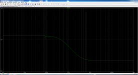
That's the output capacitor resonating with the inductive output impedance of the capacitance multiplier; the ESR provides damping. It's well worth simulating this with a realistic model of a capacitor.
That is what I was trying to do, adding parasitics to the capacitor to get more realistic results. I noticed that making the ESR really big made the curve really flat.
A 2A steady current is applied during the run.
OK, but what about a chart for class A/B load also.
Picking this back up...
OK, time to pick this back up. I mistakenly made a post in the GB section by clicking on an old thread subscription without paying attention.
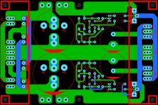
Here's a peek. It is currently a 4" x 6" (101.5mm x 152.3mm) board and can accommodate up to 40mm snap in caps with 10mm LS two pin or 22.5mm LS four pin. Comments or suggestions welcome. It isn't quite finished but should be close to its final form. There are errors on the silk that will be addressed.
There was a suggestion to chassis mount the pass devices and go dual bridge. Thoughts?
OK, time to pick this back up. I mistakenly made a post in the GB section by clicking on an old thread subscription without paying attention.
Here's a peek. It is currently a 4" x 6" (101.5mm x 152.3mm) board and can accommodate up to 40mm snap in caps with 10mm LS two pin or 22.5mm LS four pin. Comments or suggestions welcome. It isn't quite finished but should be close to its final form. There are errors on the silk that will be addressed.
There was a suggestion to chassis mount the pass devices and go dual bridge. Thoughts?
Attachments
In simulation I'm getting about -72dB ripple reduction. My 'dead bug' test circuit's output ripple was below my Tektronic TDS-210's ability to measure - just system noise visible. Real current delivery is provided by the output capacitance, 4700uF will be the suggested value. The ripple reduction is provided by 'phantom' capacitance. That is to say no capacitance multiplier can replace real capacitance, it just mimics the ripple reduction of a big bank of capacitors.
The capacitance multiplier will drop about two volts from the bulk supply (more if the ripple is high), so power dissipation becomes its voltage drop multiplied by average current through it. An average 5A draw would then have to dissipate at least 10W in the multiplier per rail.
The main limiting factors become current through the pass devices and their dissipation.
The main limiting factors become current through the pass devices and their dissipation.
A few thoughts - please accept with/without prejudice, as they say, or ignore completely!
You seem to have two channels of the power amp operating from one single output 4700uF capacitor - is this a specific design choice?
If the central 0 volt point of the amp is adjacent to the output +/- supply terminals, the 'noise' from the rectifiers and mains supply noise are passing through that large central ground 'strip' right past the track that connects to the reference circuitry - perhaps this might benefit from a change ...
Is the component next to the big caps (10,000uF?) for a current reducing series resistor? (between the diodes and the main ripple cap) - perhaps a relocation to get a possible heat source away from the electrolytic ....
There's no provision for any AC noise filters &/or snubbers, but a lot of terminals - what's intended here?
You could easily make this a single sided pcb just with a couple of links ...
A few thoughts - please accept with/without prejudice, as they say, or ignore completely!
You seem to have two channels of the power amp operating from one single output 4700uF capacitor - is this a specific design choice?
If the central 0 volt point of the amp is adjacent to the output +/- supply terminals, the 'noise' from the rectifiers and mains supply noise are passing through that large central ground 'strip' right past the track that connects to the reference circuitry - perhaps this might benefit from a change ...
Is the component next to the big caps (10,000uF?) for a current reducing series resistor? (between the diodes and the main ripple cap) - perhaps a relocation to get a possible heat source away from the electrolytic ....
There's no provision for any AC noise filters &/or snubbers, but a lot of terminals - what's intended here?
You could easily make this a single sided pcb just with a couple of links ...
I'm always open to thoughts or suggestions. As mentioned, it isn't quite complete and subject to change.
The intent is to allow one PSU to have connections for two channels. I chose to orient the connectors to allow one close-knit (twisted) group of supply wires to be run together to each amplifier rather than have all the positive connections on one side and all the negative on the other. Extra terminals, especially grounds are for other returns such as speaker returns. Snubbers could be added but with fast soft recovery diodes not likely needed.
The 4700µF caps are just to help keep the circuits output impedance low and current capability up. In reality they don't need to be that big at all. MrEvil's original design had only 100µF at the output. There is likely little benefit from going any larger, in fact it should already be over-kill.
The mystery components adjacent to the main reservoirs are for fuse holders / clips.
The routing of the ground to the actual multiplier circuit could be different. I have thought as well they should perhaps be moved towards the output lines. Not sure how critical it will be in reality.
My intent is to have boards made professionally. I avoid doing home etching these days and don't tend to design for it anymore, hence a dedicated double sided layout. I avoid links / jumpers in favour of vias and top side copper.
This supply targets the ~100W-ish class AB/B type amplifier and could be used with smaller class A designs as well. It could be scaled to higher powers. My intent for this one is to output 45-50V rails or lower. The big thing to remember that it can't do the exact same job as massive capacitor banks, namely providing huge bursts of current on demand, but is great where current requirements are low to moderate and you want the ultra low ripple only a absurd amount of capacitance could provide.
The filtering is done electronically, hence the 'Capacitance Multiplier' name. We are RC filtering the 'dirty' rail to provide a relatively smooth reference and setting the output a little lower than the bulk supply to basically throw away the ripple on the output. Generally the output will be about 2V or so lower than the bulk rails average value (a little below the ripples trough / valley).
This simplified version was simulated with 2.66Vp-p ripple in and gave 340µVp-p ripple out while delivering 4A DC, which is -78dB less ripple out relative to in. I rat's nested the positive rail and put an artificially softened supply to it and couldn't even see evidence of ripple on the oscilloscope. The more complex circuit may do better in theory, but I think this will work nicely with a very simple circuit in practice. And all this before we even introduce the amplifier's own PSRR.
Main application for this PSU is low to mid power amps that use circuit topology with low immunity to PSU induced ripple. Like VSSA and other current feedback circuits. Or for low power class A amp that draw constantly higher current from PSU. For conventional topologies with input differential pair cap multiplier is not necessary.
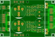
Folks seem to think it is too big? Funny, this board isn't that much bigger than what PMI was offering, but I've already had more than one comment about its size  .
.
It could be reduced in size at the expense of capacitor selection options. Almost certainly the capacitors will stand taller on the board than the pass transistors. It would be possible to make the pass devices mount under the board attached to chassis with the proviso that the chassis is aluminum.
I'm open to specific thoughts, but bear in mind that no single implementation is going to make everyone happy nor is this going to suit everyone's various needs or requirements. I'm after a generic, useful to many but not necessarily perfect for a specific application, type of project.
.It could be reduced in size at the expense of capacitor selection options. Almost certainly the capacitors will stand taller on the board than the pass transistors. It would be possible to make the pass devices mount under the board attached to chassis with the proviso that the chassis is aluminum.
I'm open to specific thoughts, but bear in mind that no single implementation is going to make everyone happy nor is this going to suit everyone's various needs or requirements. I'm after a generic, useful to many but not necessarily perfect for a specific application, type of project.
- Home
- Amplifiers
- Power Supplies
- Simplified MrEvil / PMI Capacitance Multiplier