
post1073
What does the info in white near top left mean?
I see " H 5.00us "
The wave form fills across three divisions indicating 15us, or ~67kHz
I'm not used to reading these digital sampling scopes.Maybe I'm doing something wrong with measurement setup?
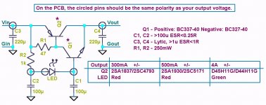
Yellow trace in IN and blue is OUT. Files names are indication condition.
How to see if it is working ok?
What does the info in white near top left mean?
I see " H 5.00us "
The wave form fills across three divisions indicating 15us, or ~67kHz
Good catch. I never know what they are saying either because often there are no labels or there is conflicting information on the screen, so I just assume the user has the scales set correctly.
67KHz sounds reasonable for a SMPS PSU like he is using. But that fact it is 100mV now and not 12mV points to a fault or something wrong with it, which makes me hesitant to focus on the KM until that is explained.
67KHz sounds reasonable for a SMPS PSU like he is using. But that fact it is 100mV now and not 12mV points to a fault or something wrong with it, which makes me hesitant to focus on the KM until that is explained.
Last edited:
It means that sample was taken in 5us/dev (5 milliseconds). In did, my buck converter is working with 60kHz switching frequency. Both channels (input and output) are x10 on probes and on scope attenuated, AC coupled and 20MHz limited. Trigger is set for mix, falling and raising edges and it is around 0v. So, I assume that my test setup is correct.
Last edited:
that does not explain what we see of the 5.00us setting for Horizontal.It means that sample was taken in 5us/dev (5 milliseconds). In did, my buck converter is working with 60kHz switching frequency. Both channels (input and output) are x10 on probes and on scope attenuated, AC coupled and 20MHz limited. Trigger is set for mix, falling and raising edges and it is around 0v. So, I assume that my test setup is correct.
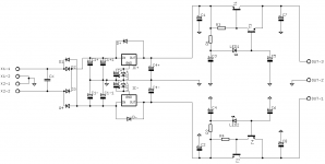
Hello Keantoken,
I was trying to make a layout for your K-mult, but before committing too much, just had a few questions. I need it for a class A HPA running on +/-15V. I just followed your circuit.
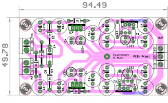
1. would making whole of top side as ground help. example of this is attached for your k-mult.
2. Would keeping this at the output of a std LM317 /337 be better than a regulator only supply
thanks and regards
Prasi
I was trying to make a layout for your K-mult, but before committing too much, just had a few questions. I need it for a class A HPA running on +/-15V. I just followed your circuit.
1. would making whole of top side as ground help. example of this is attached for your k-mult.
2. Would keeping this at the output of a std LM317 /337 be better than a regulator only supply
thanks and regards
Prasi
Attachments
I think if you could route the ground on the bottom layer in the "H" shape shown on the board, and then use a ground plane that is connected only at the input ground and nowhere else, you would have a 'good practice' implementation of a ground plane for LF.
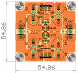
I can't figure out what the magenta on your PCB is supposed to represent. Is it a 3 layer board? Also C4 is turned around...
I can't figure out what the magenta on your PCB is supposed to represent. Is it a 3 layer board? Also C4 is turned around...
I think if you could route the ground on the bottom layer in the "H" shape shown on the board, and then use a ground plane that is connected only at the input ground and nowhere else, you would have a 'good practice' implementation of a ground plane for LF.
I can't figure out what the magenta on your PCB is supposed to represent. Is it a 3 layer board? Also C4 is turned around...
Its a 2 layer board only
refering to the earlier attached image , The dark brown colored traces are the signal and the khakhi plane is the ground plane which covers the entire board on top side.
here is the exact schema. I think C4 is correct.
the second image is with the ground plane ripped, so all the pads with a white hollow around them are connected to ground.Hope this image helps.
Attachments
C4 is electrically correct but breaks the pattern of symmetry... I guess it doesn't matter.
Keep in mind I've only made a few PCBs in my life. That said, I'm pretty sure what I already described will work.
The problem with connecting all capacitor grounds to a ground plane is that the currents may wander to different parts of the plane and disrupt circuitry in ways that are hard to predict. Honestly I don't think there would be any problem with this circuit except in extreme cases, but what I described is the safe option.
C4 is electrically correct but breaks the pattern of symmetry... I guess it doesn't matter.
Keep in mind I've only made a few PCBs in my life. That said, I'm pretty sure what I already described will work.
The problem with connecting all capacitor grounds to a ground plane is that the currents may wander to different parts of the plane and disrupt circuitry in ways that are hard to predict. Honestly I don't think there would be any problem with this circuit except in extreme cases, but what I described is the safe option.
Thank you,
here is take 2, but with regulator added upfront.
All ground traces run to a point where k-mult input GND would be if it were on a separate PCB.
Would it be advisable to make a ground plane just for the regulator and diode section then run a single track to the k-mult star ground?
regards
Prasi
Attachments
Prasi,Thank you,
here is take 2, but with regulator added upfront.
All ground traces run to a point where k-mult input GND would be if it were on a separate PCB.
Would it be advisable to make a ground plane just for the regulator and diode section then run a single track to the k-mult star ground?
regards
Prasi
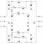
your schematic is going to mislead you into making connections in the wrong places.
The centre tap of the transformer must connect to the junction between C1+ and C1-
Remove the ground symbol just to the right of C1+1/C1-1
The regulator reference connects through C+ and LED+, the lower end of this pair connect to C4+. This junction becomes the main zero volts reference for all the output currents. This could be on your zero volts power plane.
Last edited:
- Home
- Amplifiers
- Power Supplies
- Keantoken's CFP cap multiplier