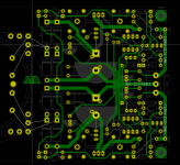
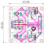
If you insert space between your heatsink and the board then you're relying on the bottom pad (plus whatever small amount of solder wicks to the top) to hold it. That's a pretty tall heatsink for that.
I'd move the top copper traces a little so they aren't under the heatsink, and then mount the heatsink flush to the board.
good thinking I can do that
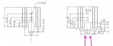
") I think I can then change the traces so that they are gonna be under this space so is not gonna get in contact with the heat sink I have like about 11mm of space the traces are 0.80mm
I think I can then change the traces so that they are gonna be under this space so is not gonna get in contact with the heat sink I have like about 11mm of space the traces are 0.80mmAttachments
What's the intended purpose of the added copper in post #238?
oh I was just asking if that is a good idea or not
ok so this is how much space I can get about 11mm I need to move those traces away from the heat sink footprint
Attachments
Don't count on the heatsink being machined with tight tolerances. You'd still got plenty of room; I'm just saying I'd stay to the middle 8mm-ish, rather than trying to use all 11.1mm.
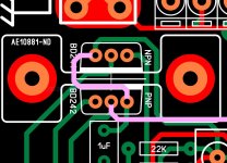
Also note that the lower purple trace goes under the fins as it exits to the right of that last picture....
Also note that the lower purple trace goes under the fins as it exits to the right of that last picture....
Don't count on the heatsink being machined with tight tolerances. You'd still got plenty of room; I'm just saying I'd stay to the middle 8mm-ish, rather than trying to use all 11.1mm.
Also note that the lower purple trace goes under the fins as it exits to the right of that last picture....
got it
Attachments

Don't you think the power traces are too thin?
And one more, much important note - in order to not compromise the capabilities of this not bad schematic, you must have a point connected to the GND net which to serve as a reference ground for the error amplifiers - otherwise performance will be left on the paper only.
And one more, much important note - in order to not compromise the capabilities of this not bad schematic, you must have a point connected to the GND net which to serve as a reference ground for the error amplifiers - otherwise performance will be left on the paper only.
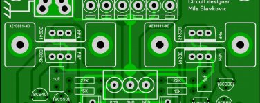
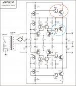
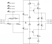
The series regulator (circled in red) is a Sziklai pair. They can be prone to oscillation. The traces shaded in red inside the circle must be kept short.
The shunt regulator (circled in blue) is an emitter-follower. It suffers no oscillation issues, so the trace lengths there don't matter much. (Sadly, those are the ones that you have nice and short.)
Same for the bottom half of the regulator.

The shunt regulator (circled in blue) is an emitter-follower. It suffers no oscillation issues, so the trace lengths there don't matter much. (Sadly, those are the ones that you have nice and short.)
Same for the bottom half of the regulator.
Attachments
I'm gonna take a break I been checking this layout for way too long I will continue tomorrow I'm too burned out
These things take time. The guy that lead me through my first layout had a tag-line which read "everything matters". Sadly, it's more true than not.
Jeff, with all my respect - the top of schematic is not series regulator - this a CCS (constant current source). The bottom part is the error amplifier with the regulation element. And when I'm speaking about the common reference ground, I'm not worrying about stability but for the PSRR itself. As any error tracking amplifier, the lower part of schematic has a voltage reference and negative feedback network. They (at least) must be connected with independent traces in one point which is the ground reference. This is the summing point for the currents flowing from the two big electrolytic capacitors and sinking to the output.
BTW, stability is an issue which must not be leaved aside - and curiously, all my problems with oscillations in the shunt regulators are caused by the CCSses, not by the part of schematic with NFB (well, the current sources were much more sophisticated than this one).
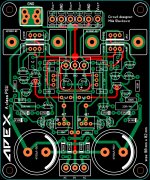
I'm attaching a picture with partly finished regulator in order to explain what I'm talking about (well, it could be too exaggerated but better exaggerated than underperformed).
BTW, stability is an issue which must not be leaved aside - and curiously, all my problems with oscillations in the shunt regulators are caused by the CCSses, not by the part of schematic with NFB (well, the current sources were much more sophisticated than this one
).I'm attaching a picture with partly finished regulator in order to explain what I'm talking about (well, it could be too exaggerated but better exaggerated than underperformed
).Attachments
Last edited:
Jeff, with all my respect - the top of schematic is not series regulator - this a CCS (constant current source).
Agreed. I meant "series element", but CCS is a more complete description.
The bottom part is the error amplifier with the regulation element. And when I'm speaking about the common reference ground, I'm not worrying about stability but for the PSRR itself. As any error tracking amplifier, the lower part of schematic has a voltage reference and negative feedback network. They (at least) must be connected with independent traces in one point which is the ground reference. This is the summing point for the currents flowing from the two big electrolytic capacitors and sinking to the output.
We're in (slightly) less agreement here. The only large currents are those being dumped by the shunt element and returned from the output. The variable-CCS-fed 15K resistor forming the voltage reference, and the 22K/15K voltage divider for the feedback don't dump enough current to produce much of a voltage delta on the 0-volt trace.
So, for me, I'd be happy enough with the output and shunt return sharing a 0-volt trace, and the voltage reference and voltage divider sharing a 0-volt trace. But I do agree that having all 4 share a single 0-volt trace is going to throw away some performance.
BTW, stability is an issue which must not be leaved aside - and curiously, all my problems with oscillations in the shunt regulators are caused by the CCSses, not by the part of schematic with NFB (well, the current sources were much more sophisticated than this one
I'm attaching a picture with partly finished regulator in order to explain what I'm talking about (well, it could be too exaggerated but better exaggerated than underperformed
Yeah, this is one of the reasons I don't like ground-planes. They tend to make people lazy and not think through their return current paths. (That being said, I do still use them sometimes.)
Cheers,
Jeff.
The question is not about the current through the voltage divider but to which point it will be connected to the ground net - if this point is different than the point of connection of the voltage reference and suppose through the trace which connects them flows the big return regulator's current, any change in current consumption will lead this two points to bounce. This will compromise schematic's performance.
The question is not about the current through the voltage divider but to which point it will be connected to the ground net - if this point is different than the point of connection of the voltage reference and suppose through the trace which connects them flows the big return regulator's current, any change in current consumption will lead this two points to bounce. This will compromise schematic's performance.
I'm completely in agreement if the bolded part is true. I'm just saying that if you separate that out, then it'd be good enough for me.
Cheers,
Jeff.
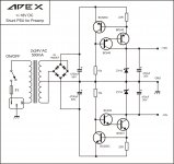
Simple Shunt PSU for Preamps
Hello, does anyone have PCB thermal transfer?
Attachments
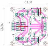
something i made just now.
Thank you Prasi, very agile, do you have the pdf file for thermal transfer?
here you go. they are mirrors. is it ok?
PS main caps are 20 mm dia and output caps are 13mm dia.
Yes, it's ok, thank

- Home
- Amplifiers
- Power Supplies
- A-class Preamp PSU