Can't say if it will work stably just theoretically. It has a compound output that makes it demanding. That's a major difference. I would not use R13 at all if not using C2.Hello Salas
I am revisiting the V12R shunt because I do know it's potential and would like to push it a little further.
The initial schematic is below and I would like to drop C2 (47uF EL).
I know the BiB and the folded shunt can both work perfectly without that output EL.
The différences I see are related with the resistor value in the output zobel that in the BiB is 1.2ohm and in the V12R is 0.22 ohm.
Can I take the V12R schematic, drop the output EL and raise the zobel resistor to 1.2ohm and expect it to work without oscilations ?
Do you realise that Vp of Q9 should be less than 50% of Vbe of Q7.
That would require R12 to be VERY low and for Idss of Q9 to be selected from the low end of gr grade sk170.
Reducing Id of a bl grade sk170 by using a high value for VR12 is not a good way of getting good performance from that transistor.
If trimming to a preferred voltage is required, then the VR could be moved to be in series with R11.
Its an old schematic based on certain characteristics of stashed samples that worked in a prototype. Due substitutions of types can be made but it takes practical work to confirm good working order and stability. Using a VR "upstairs" its a correct idea, I had confirmed it was OK combined with low side K117GR too in another proto. But keep R11 high value enough for C1 ro remain effective in LF. Vp must not be more than 100% of Q7 Vbe actually since its a minus Vp. So to confirm to the no less VDS than double the Vp criterion.
Do you realise that Vp of Q9 should be less than 50% of Vbe of Q7......................
I think you have two concepts mixed up....................... Vp must not be more than 100% of Q7 Vbe actually since its a minus Vp. So to confirm to the no less VDS than double the Vp criterion.
To work effectively the lowest jFET must be constant current.
That happens when Vp<50% of the applied Vds.
The Vds is from the Vbe of the BJT.
Thus Vp<50% of Vbe.
yet you said "Vp must not be more than 100% of Q7 Vbe".
Surely you did not mean that?
I think you have two concepts mixed up.
To work effectively the lowest jFET must be constant current.
That happens when Vp<50% of the applied Vds.
The Vds is from the Vbe of the BJT.
Thus Vp<50% of Vbe.
yet you said "Vp must not be more than 100% of Q7 Vbe".
Surely you did not mean that?
What I meant with "since its a minus Vp" is that the absolute value of Vp can be up to the same as Vbe. Since the NJFET has -Vp and BJT NPN Vbe is positive, then 0.65V Vbe is two times away to -0.65V Vp as a distance for example. So |Vp| can be up to equal |Vbe| i.e. up to 100% in absolute value to meet the criterion.
No.
The -ve Vgs tells us that the voltage at the Source of an NjFET is above the voltage at the Gate.
i.e. the V measured at the gate using the source as reference is a -ve value.
If the Vgs when near zero current is passing is -0.65Vgs then that means the Source voltage is actually higher than the gate voltage.
But the Vds is the value that should be at least double the Vp for effective CCS action.
The Vds + the source resistor voltage drop equals the Vbe of the transistor.
If the resistor is a non zero value then it becomes even more difficult to achieve Vp~=Vbe/2
Try the experiment.
Connect G to S as you would for measuring Idss.
Apply a 10V Vds. Measure the current.
reduce Vds in steps and remeasure the current.
Keep reducing Vds to ~ Vp.
Now plot the Ic vs Vds.
You will find that Ic holds very close to CCS when Vds is >5Vds
From 5Vds down to 2*Vp, the Ic falls as CCS action gets worse.
From 2*Vp down to 1*Vp, the Ic falls so badly that one can no longer call the jFET a CCS. It behaves as a low value resistor.
Last edited:
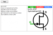
A low Idss sk170 of 3mA will have a Vp of around 200mV to 300mV
This would work well as a CCS under a Vbe of around 600mVbe
Instead choose a 6mA sk170 where Vp could be around 300mV to 400mV.
When that is under a 600mVbe it will not perform as well.
Now choose a middle of the BL range sk170. It will have a Vp that is too high to be an effective CCS under a 600 to 700Vbe.
Putting in a source resistor to reduce Ic helps a little bit. But not nearly enough. It is FAR BETTER to select a low Idss NjFET.
The Borbely rule of Vds >= 2*Vp guides us. Use it.
Last edited:
That seems sound. These short-channel devices are handy for many things but do have a rather high output conductance for current generator use.The Borbely rule of Vds >= 2*Vp guides us. Use it.
The circuit works, so I don't want to get too far into this, and bipolars do have advantages in many places compared to FETs, but I might try replacing this one with an enhancement mode DMOS, as the gate-source voltage will be a few volts and allow the JFET to perform better. Also the impedance at that node will be much higher than a forward-biased base-emitter junction. One would not use a very low threshold voltage DMOS part, but something along the lines of the 2N7000.
Brad
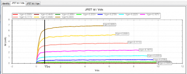
This is a -0.47V pinch off K170BL example I just traced out. Although even straighter later, it looks usable above Vbe=Vds. Its Ohmic region already gives way to the saturation region when under Vbe voltage only in other words.
Attachments
That seems sound. These short-channel devices are handy for many things but do have a rather high output conductance for current generator use.
The circuit works, so I don't want to get too far into this, and bipolars do have advantages in many places compared to FETs, but I might try replacing this one with an enhancement mode DMOS, as the gate-source voltage will be a few volts and allow the JFET to perform better. Also the impedance at that node will be much higher than a forward-biased base-emitter junction. One would not use a very low threshold voltage DMOS part, but something along the lines of the 2N7000.
Brad
Noise issues concerned? When looking to keep the noise spec the same as before I mean.
Yes, that certainly is a consideration. Unfortunately noise is rarely specified for MOS, especially low-frequency excess noise. I'm amazed by how good some of the DMOS op amps are, but they still have a significant rise at lower frequencies.Noise issues concerned? When looking to keep the noise spec the same as before I mean.
Try the experiment.
Connect G to S as you would for measuring Idss.
Apply a 10V Vds. Measure the current.
reduce Vds in steps and remeasure the current.
Keep reducing Vds to ~ Vp.
Now plot the Ic vs Vds.
You will find that Ic holds very close to CCS when Vds is >5Vds
From 5Vds down to 2*Vp, the Ic falls as CCS action gets worse.
From 2*Vp down to 1*Vp, the Ic falls so badly that one can no longer call the jFET a CCS. It behaves as a low value resistor.
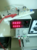
I tried the experiment for that same -0.47V Vp K170BL. A jumper between G & S. A variable PSU for VDS. The thick red lead in the picture goes to a Fluke 87V in series mA DC mode for better readings than the PSU's at this difficult for its resolution region.
VDS / Id
10V 7.20mA
4.0V 6.93mA
1.0V 6.39mA (at about 2*Vp)
0.7V 6.17mA (at about Vbe)
0.5V 5.83mA (at about 1*Vp)
0.3V 4.84mA
So 9.6% current fall between 2*Vp and 1*Vp at Vgs=0
Attachments
I'm curious as to the function of R10---was it needed for stability?Yes, that certainly is a consideration. Unfortunately noise is rarely specified for MOS, especially low-frequency excess noise. I'm amazed by how good some of the DMOS op amps are, but they still have a significant rise at lower frequencies.
In any event, one concern I'd have is when the output might be inadvertently shorted to common, as C1 will break down the Q7 base-emitter junction, although this will be to some extent reduced by the action of Q9. A reverse-biased diode from the base to common would protect against beta degradation---of course one could simply never short the output.
Back to noise: the circuit response to Q9 and R12 noise is that of a first-order lowpass rolloff commencing at about 0.8Hz, with a low frequency gain of about 37dB (set by R11 and C1). For a ~1nV/sq rt Hz JFET and R12 equal to 523 ohms, this may amount to about 250nV rms at the reg output (very good indeed). The larger contribution will be from Q7 and R10, which have a noise gain of about unity out to fairly high frequencies. At the operating point of Q7 of a few mA Ic, the Q7 voltage noise should be dominated by rbb'---but the 1k of R10 will swamp this, hence e sub n of Q7 can practically be ignored. In a 20kHz noise bandwidth the output noise due to R10 should be about 141 times R10 noise, or about 575nV rms at 300K. Shot and excess noise in Q7 Ib will probably contribute about as much (in a 20kHz noise bandwidth for pure shot noise and an Ib of 9.4uA, about 266nV rms, but base current noise is usually a good deal higher than just that due to shot noise). So the transistor and R10 will dominate the noise, most likely. It could be reduced a good deal by eliminating R10.
As far as DMOS in that spot goes, for my 2N7000 model the output impedance of the circuit is lower at low frequencies but doesn't stay as low as the bipolar version, starting to climb above about 1kHz. As far as noise, I don't know how current parts are doing, so it is hard to predict, although it is probably pretty decent above a kilohertz.
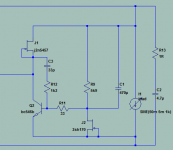
Ok, I will move VR12 up and also put a led in series with it as you use on the folded.
As for Q9 Vp < 50% Q7 Vbe maybe I could raise this Vbe up by using a diode as emitter for Q7 ?
You probably can but it has a resistance delta and some own noise. I would nest a low side Idss K117GR instead.
Winfield Hill's measurements of 2N7000s a while back sound pretty pessimistic: see Noise performance of small package mosfets | Electronics Forums
The disparity between that and what is being achieved in op amps is striking!
The disparity between that and what is being achieved in op amps is striking!
Here it is when using a moderate 220uF across Rref filter. Can take 1000uF with no problem. An Audio Precision analyzer station was used. The orange dotted line is the V1.1
http://linearaudionet.solide-ict.nl/sites/linearaudio.net/files/V4 JW F7.pdf
http://linearaudionet.solide-ict.nl/sites/linearaudio.net/files/V4 JW F7.pdf
- Status
- This old topic is closed. If you want to reopen this topic, contact a moderator using the "Report Post" button.
- Home
- Amplifiers
- Power Supplies
- The simplistic Salas low voltage shunt regulator