off topic
I just listened to the first few bars of "temptation" (Athens audiophile).
I don't have the original in any format, but I can tell you that the quality coming from disco speakers (15"+compression horn) is far better than YouTube can provide.
Why do you tubers think they can demonstrate Audio Quality via that medium?
ikoflexer said:Oooooh! I'd say between 40 and 49. Can you recommend smth?
Edit: I'm about to go for a v-strom ride in the rain, so... I'm looking forward to your answer when I'm there.")
They say good words for the Elsinore and I guess its right for your space.
Re: off topic
At least in that video it was something like a tribute to the dreamer audiophile. I have seen other videos though that a guy says ''here is my new speaker'' and others comment ''Good! I can say even from the video''. Just enthusiasm I guess.
AndrewT said:I just listened to the first few bars of "temptation" (Athens audiophile).
I don't have the original in any format, but I can tell you that the quality coming from disco speakers (15"+compression horn) is far better than YouTube can provide.
Why do you tubers think they can demonstrate Audio Quality via that medium?
At least in that video it was something like a tribute to the dreamer audiophile. I have seen other videos though that a guy says ''here is my new speaker'' and others comment ''Good! I can say even from the video''. Just enthusiasm I guess.
HI IKO my suggestion http://www.quarter-wave.com/Project08/Project08.html
Hi Ikoflexer,
great to see you latest results. It's always ensuring when practice and theory are in line.
As you write it's fun to do this exercise and it extends our understanding.
I think you can even further simplify the remote sensing, by leaving J2 and J3 in the shunt part, on the left side ground/supply. These are merely current sources, so "should not have a notion of voltage". That way you only have 2 components (ZT and Q3) as the remote sense.
Elaborating further on the idea of having dedicated shunts for each circuit stage, you can just put multiple transistors for Q1. Currents will not be matching exact, but that's not important here, since the excess current is shunted anyway. So the amount of extra components is minimal, one extra Q1 per dedicated shunt stage. Combined with remote sensing, it can still be a modular/scalable design. For example make provision for 4 shunts, what's not needed you simply don't mount on the PCB.
I don't know if this brings some sonic value though, but just for the record.
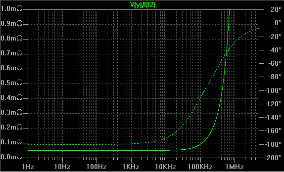
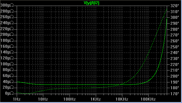
How do you test stability? Do you use a transient step response and observe the ringing?
JP.
great to see you latest results. It's always ensuring when practice and theory are in line.
As you write it's fun to do this exercise and it extends our understanding.
I think you can even further simplify the remote sensing, by leaving J2 and J3 in the shunt part, on the left side ground/supply. These are merely current sources, so "should not have a notion of voltage". That way you only have 2 components (ZT and Q3) as the remote sense.
Elaborating further on the idea of having dedicated shunts for each circuit stage, you can just put multiple transistors for Q1. Currents will not be matching exact, but that's not important here, since the excess current is shunted anyway. So the amount of extra components is minimal, one extra Q1 per dedicated shunt stage. Combined with remote sensing, it can still be a modular/scalable design. For example make provision for 4 shunts, what's not needed you simply don't mount on the PCB.
I don't know if this brings some sonic value though, but just for the record.
How do you test stability? Do you use a transient step response and observe the ringing?
JP.
ikoflexer said:Elsinore?Yeah, but then I have to build a serious power amp. You see how one can end up like those guys in the video? Slippery slope isn't it?
Just a couple of Hypex ready made modules and you are done.
Attachments
I saw the passive, did not like it. I prefer to have a processor because they will misbehave when going so low in less than huge rooms.
That little Jordan + Alcone 8 inch was a project for a friend, the drivers he bought and remain boxed and he is after gf, never made the cabinet. But I will get him sooner or later!
That little Jordan + Alcone 8 inch was a project for a friend, the drivers he bought and remain boxed and he is after gf, never made the cabinet. But I will get him sooner or later!
Ot helps software
this helps for found a resistor value from // http://rval.smartcode.com/info.html
ps OB not energized too much room mode
this helps for found a resistor value from // http://rval.smartcode.com/info.html
ps OB not energized too much room mode
jeepee said:
How do you test stability? Do you use a transient step response and observe the ringing?
JP.
Transient analysis (with careful attention to settings maximize accuracy) and phase margin analysis on all gain loops. If those tests pass under a number of conditions (various load and input voltage functions to stress it) then, if the circuit is promising, I prototype it and test it in the real world.
Hi Ikoflexer,
your stability analysis sounds very thorough, well done. Despite phase/gain margin theory I've always felt transient step response to be more revealing.
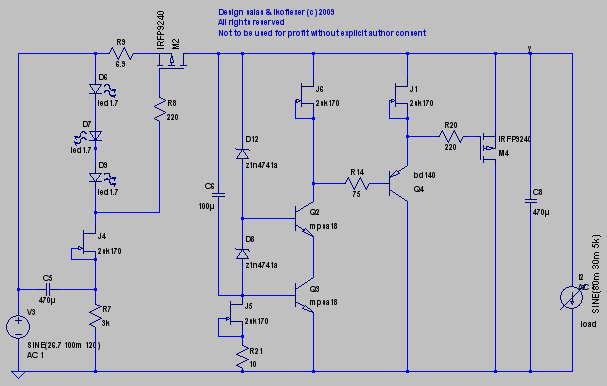
I don't think this is really a measurement bridge, since J2/J3 are current sources.
J2 provides a bias to DZ, nothing more. It could be replaced by a resistor, since Q3 keeps the voltage across it nearly constant. J3 is a current source to bias Q3, but at the same time provides a high impedance to achieve lots of (loop)gain to control M3 gate (was Q4?). If you would replace it with a resistor (in your mind), then you would see that it should be connected from M3's gate to M3's source. When connected to the far-away-load, it would directly influence the (loop)gain of Q3...
Since J2/J3 have higher impedance than a resistor, for the same current, the connection scheme would be more or less equivalent in performance.
JP
your stability analysis sounds very thorough, well done. Despite phase/gain margin theory I've always felt transient step response to be more revealing.
AndrewT said:J2 & J3 are part of the measuring bridge.
I don't think this is really a measurement bridge, since J2/J3 are current sources.
J2 provides a bias to DZ, nothing more. It could be replaced by a resistor, since Q3 keeps the voltage across it nearly constant. J3 is a current source to bias Q3, but at the same time provides a high impedance to achieve lots of (loop)gain to control M3 gate (was Q4?). If you would replace it with a resistor (in your mind), then you would see that it should be connected from M3's gate to M3's source. When connected to the far-away-load, it would directly influence the (loop)gain of Q3...
Since J2/J3 have higher impedance than a resistor, for the same current, the connection scheme would be more or less equivalent in performance.
JP
Hi,
do that mind game, replace the two CCSs with resistors.
Look again at the measuring bridge.
The node on one side provides a reference voltage.
The node on the other side divides down the output voltage. The low power transistor compares the two voltages and outputs an error voltage to the gate of the shunt.
It is a measuring bridge, it matters not that the legs have resistors replaced with CCSs to improve the performance of the circuit.
Now, go further.
Take the reference voltage leg and separate it from the dividing leg.
Connect the ref. voltage leg to a raw DC supply.
Apply a voltage modulation to the top or bottom end of the ref. voltage leg.
Will the circuit detect the modulation as an error and apply a correction to feed to the shunt? What if the ref leg is connected to the wrong node?
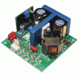
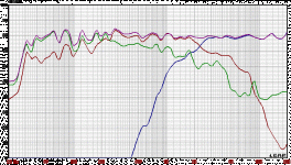
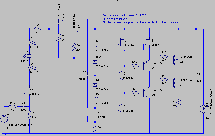
JP, Andrew, gentlemen, if you would be so kind to have a look at this circuit. This is currently implemented in my living room and stable, using exactly the parts in the schematic. The simulation shows good performance. In practice it looks good too, but I have not done detailed performance tests. I have a few variations with even much better simulated performance but in practice they were oscillating like crazy.
The change from salas' original circuit is small, moved to cascode followed by a buffer. My intention was to lower the output impedance a bit and also to extend its bandwidth.
Thanks for a stimulating discussion!
The change from salas' original circuit is small, moved to cascode followed by a buffer. My intention was to lower the output impedance a bit and also to extend its bandwidth.
Thanks for a stimulating discussion!
One thing I like about this circuit is not only its performance, but its extendibility. For instance I've wanted a high voltage high(ish) current regulator for my headphone amp. salas has already built a HV version of v1, but I had problems getting it to work for a higher current. I think the mosfet SOA is not very optimistic for continuous high current. Please feel free to disagree; my parts cemetery was my experience. To address this I would/will probably implement something like the following.
One thing I don't have experience with is how to protect the parts at high voltage and possibly against high inrush current? Zeners to protect the mosfets of overvoltage? PTC on the input?
Any suggestions?
One thing I don't have experience with is how to protect the parts at high voltage and possibly against high inrush current? Zeners to protect the mosfets of overvoltage? PTC on the input?
Any suggestions?
M2, the CCS pass element, provides the inrush protection.
It is designed to limit the maximum current into the circuit to it's set value.
Check the dissipation on this device at switch on, i.e. maximum voltage at the input and zero voltage on the +ve rail.
The 9240 should be able to survive an ampere with a 50V input for the very few seconds it takes to charge up all the capacitors that follow the CCS.
Check the dissipation in M1 and M4. They will have different Vds but the same Id.
R1 should allow you to check Id.
Is there a possibility that oscillation is causing the failure rather than over current?
Gate voltage protection Zeners? Where are they? Vgs < Vgs max ALWAYS even during start up, shorting out, shut down, etc.
- Status
- This old topic is closed. If you want to reopen this topic, contact a moderator using the "Report Post" button.
- Home
- Amplifiers
- Power Supplies
- The simplistic Salas low voltage shunt regulator