PCB update
i have updated the PCB design. In the star ground version i widened the traces between the input and output caps. I also attempted a version using a ground plane. Both versions have wider traces for the resistor divider network that sets the output voltage.
Comments regarding the different performance characteristics of these two designs would be most welcome. Thanks.
Hi Marc,
1. for the PCB with the ground plane is there any locations that you would recommend using "strategic cuts" in the ground plane to guide currents?
2. If i were to connect the adjust pin ground on board, what would be the best location?
i ordered parts this week, if i can settle on a pcb design i should be able to get them within a couple of days.
thanks for your help,
Tim
hi,
some thoughts, if you put the main GND plane on the bottom side it give you all the top side for main power tracks and any star gounds that may be required. A standard commercal PSU would have the following format Input connectors, Circuitry, Output connectors. There is a reason for this topography, that within a power supply you generaly have internal control currents flowing that are intimate to how it performs its voltage regulation. In theory there is not one ultimate ground in a power supply like there is in an amp. You have the input GND and the output GND, and these need to be at the same potential at all times, in between these two points you have all the internal workings of the power supply (on switched mode you have some horendas current loops to control). Bakmeel siad similar things about a bottom layer contigous GND plane earler and I'd be interested in his comments now. Having not yet found any application notes for this chip yet I have to question the best GND paths for the feedback resistors bypass capacitors, as it recomends the resistor be tied to as close to the load as possible. Still thinking on that one.
some thoughts, if you put the main GND plane on the bottom side it give you all the top side for main power tracks and any star gounds that may be required. A standard commercal PSU would have the following format Input connectors, Circuitry, Output connectors. There is a reason for this topography, that within a power supply you generaly have internal control currents flowing that are intimate to how it performs its voltage regulation. In theory there is not one ultimate ground in a power supply like there is in an amp. You have the input GND and the output GND, and these need to be at the same potential at all times, in between these two points you have all the internal workings of the power supply (on switched mode you have some horendas current loops to control). Bakmeel siad similar things about a bottom layer contigous GND plane earler and I'd be interested in his comments now. Having not yet found any application notes for this chip yet I have to question the best GND paths for the feedback resistors bypass capacitors, as it recomends the resistor be tied to as close to the load as possible. Still thinking on that one.
Hi Marc,
thanks for your continued help. i hope the holiday was good.
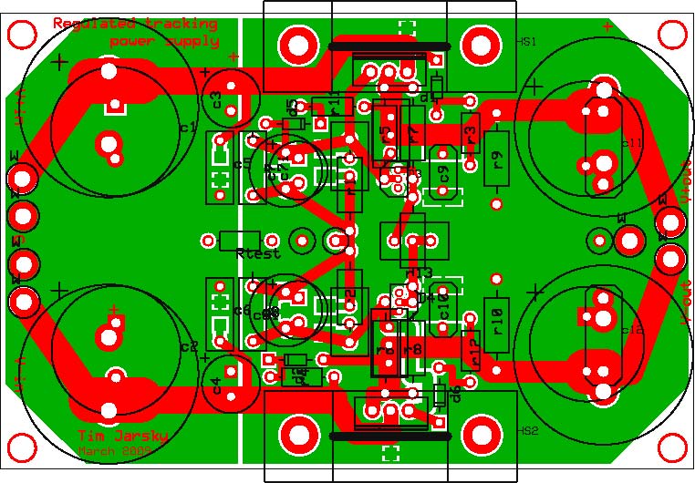
tonight i think i am going to try some major changes to the pcb layout.
One option i am going to explore is to see if i can configure it so that the input and output caps are side by side. This will hopefully ensure they are at a similar voltage.
I may also try and get the small output bypass cap much closer to the chip pins.
In regards to the ground path of the feedback resistors, if i have a on board connection, it would seem to make sense to connect it at the output as this is where the greatest load would be. I should at least include the option of connecting it there so i can test its effect.
I can now see why multilayer boards are use - even with this simple design i can see an advantage. With just one layer left for all power tracks, and the pin arrangement of the regulator, it becomes difficult to avoid crossing tracks.
Tim
thanks for your continued help. i hope the holiday was good.
tonight i think i am going to try some major changes to the pcb layout.
One option i am going to explore is to see if i can configure it so that the input and output caps are side by side. This will hopefully ensure they are at a similar voltage.
I may also try and get the small output bypass cap much closer to the chip pins.
In regards to the ground path of the feedback resistors, if i have a on board connection, it would seem to make sense to connect it at the output as this is where the greatest load would be. I should at least include the option of connecting it there so i can test its effect.
I can now see why multilayer boards are use - even with this simple design i can see an advantage. With just one layer left for all power tracks, and the pin arrangement of the regulator, it becomes difficult to avoid crossing tracks.
Tim
PCB update
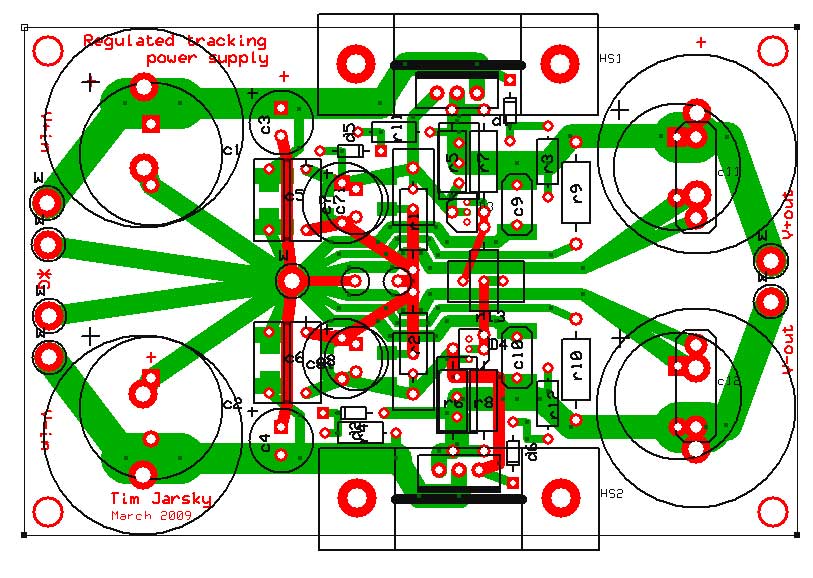
I think i am coming close to the final PCB design.
One goal of this board was to leave room for experimentation. That is why the ground plane is sliced between the main filter caps and the regulated side. I plan on investigating the differences in regulation and noise while attaching the two planes in different ways: a single connection at the center of the planes, only at the outer edges, across the entire slice, and possibly a resistor - just to push things to the extreme.
My thoughts are also clearer in regards to the adjust pin ground. By attaching the adjust pin ground off board, at the site of greatest load, i will be isolating them from the high currents moving in the ground plane of the power supply board. The effect of the off-board connection is testable and that is what i plan to do, i just hope my test gear has the resolution to resolve any differences.
One additional change was the addition of some surface mount pads very close to the regulator input pins. I hope to be able to significantly knock noise levels down with these in place.
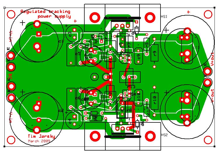
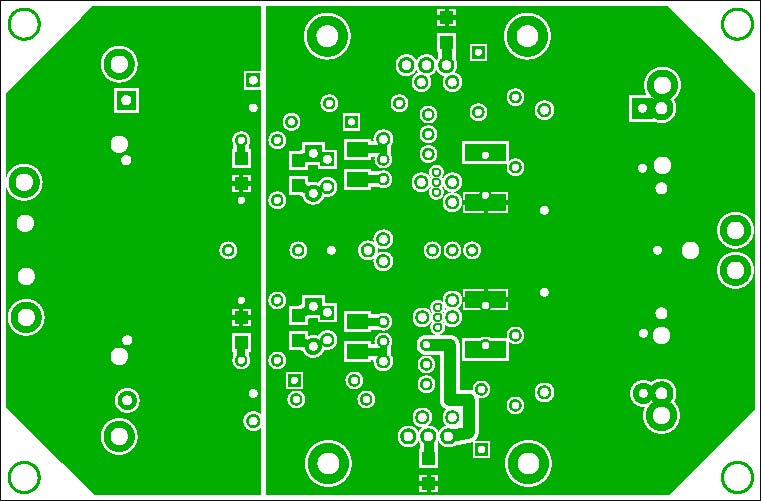
here is the PCB - all layers, top, bottom, respectively.
I think i am coming close to the final PCB design.
One goal of this board was to leave room for experimentation. That is why the ground plane is sliced between the main filter caps and the regulated side. I plan on investigating the differences in regulation and noise while attaching the two planes in different ways: a single connection at the center of the planes, only at the outer edges, across the entire slice, and possibly a resistor - just to push things to the extreme.
My thoughts are also clearer in regards to the adjust pin ground. By attaching the adjust pin ground off board, at the site of greatest load, i will be isolating them from the high currents moving in the ground plane of the power supply board. The effect of the off-board connection is testable and that is what i plan to do, i just hope my test gear has the resolution to resolve any differences.
One additional change was the addition of some surface mount pads very close to the regulator input pins. I hope to be able to significantly knock noise levels down with these in place.
here is the PCB - all layers, top, bottom, respectively.
Hi,
quick reply cos my internet is unwell at home, so I'm limited to lunch break at work!
Some more interesting links, the reason no real data is the device is not reccomended for new designs, so it will disapear in a few years.
http://www.linear.com/pc/productDetail.jsp?navId=H0,C1,C1003,C1040,C1019,P1239
http://www.linear.com/pc/downloadDocument.do?navId=H0,C1,C1003,C1040,C1019,P1239,D4133
http://www.linear.com/pc/productDetail.jsp?navId=H0,C1,C1003,C1040,C1019,P1465
http://www.linear.com/pc/downloadDocument.do?navId=H0,C1,C1003,C1040,C1019,P1465,D4137
With reference to the ground currents, cos of the frequency of most of the signals with this device, all return currents will generaly follow the path of least resistance.
Hope to be back on line soon.
hi,
back on line.
Firstly, drop us an email as I am collating some of my numerous notes on GROUND into a zip file which will provide some interesting reading and more understanding of how it all works.
I dont know how far you PS is going to be from the load, but personaly I would take the ADJ pin ground to your output connector (ie keep it on the board), as any wires to your load become part of that same load, and there is the possibility of creating more problems (any wire connection is gonna have inductance and resistance and increased loop distance). Though you could cater for both then experiment with different topographys, ie put a track to the output connector with some jumper pads so you can try a wire to the far point of load or wire across the jumpers to use the track to the output connector.
Think of the split in your ground plane like the narrow point in an hour glass just a thought.
Marc
back on line.
Firstly, drop us an email as I am collating some of my numerous notes on GROUND into a zip file which will provide some interesting reading and more understanding of how it all works.
I dont know how far you PS is going to be from the load, but personaly I would take the ADJ pin ground to your output connector (ie keep it on the board), as any wires to your load become part of that same load, and there is the possibility of creating more problems (any wire connection is gonna have inductance and resistance and increased loop distance). Though you could cater for both then experiment with different topographys, ie put a track to the output connector with some jumper pads so you can try a wire to the far point of load or wire across the jumpers to use the track to the output connector.
Think of the split in your ground plane like the narrow point in an hour glass
just a thought.Marc
Hi Marc,
i am definitely thinking about the connection between the two ground planes as an hour glass. By doing it this way i was hoping to investigate the relationship between output noise and regulation. I expect with one continuous plane, regulation would be better but output noise might be greater. If one continuous plane turns out to be best, i can easily make a continuous connection between the two planes to create a single plane.
i was aware that the lt1033 is no longer recommended for new designs. I went with it because it is a slightly better part than the lm337 and it can handle higher current loads. Also, it uses a standard 3 pin configuration making my board compatible with other 3 pin adjustable regulators. The 1185 is a 5 pin device - i actually have a couple on hand.
I have included a couple of options for hooking the adjust pin ground on board as you suggested (have not posted the final pcb tweaks yet). I actually ordered the boards last night and the parts order arrived last friday so i should be ready for testing by this weekend.
thanks again,
Tim
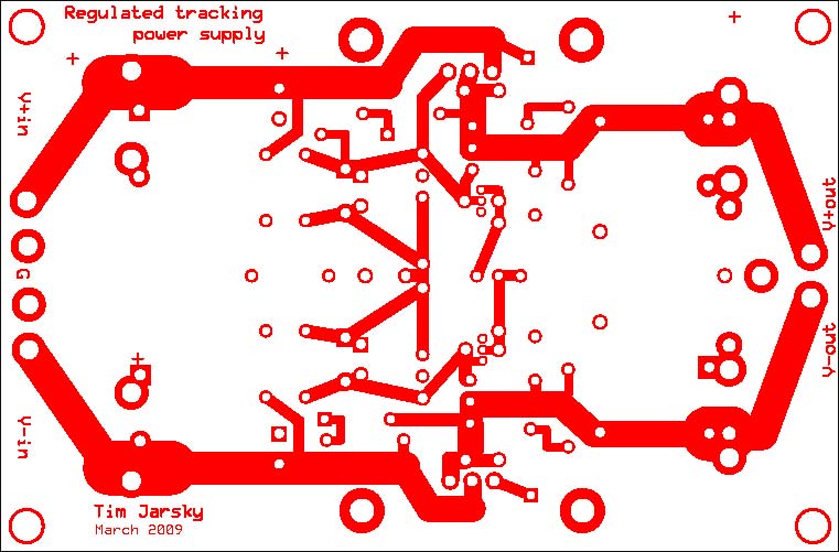
Boards arrived today. They look pretty good. Unfortunately, since ordering, i think i have learned of a better way to layout the board using separate planes for the V+in, V-in, V+out, and V-out, not just the ground. I don't know why i did not think of this before. Nevertheless, i think they should allow me to do all the experimenting i want and in the future i can always order another set. I'll post images of the updated layout later.
In the mean time here are some pics of the PCBs:
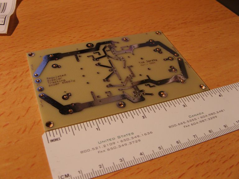
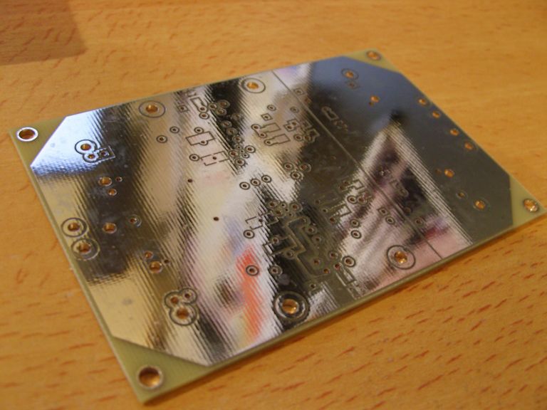
In the mean time here are some pics of the PCBs:
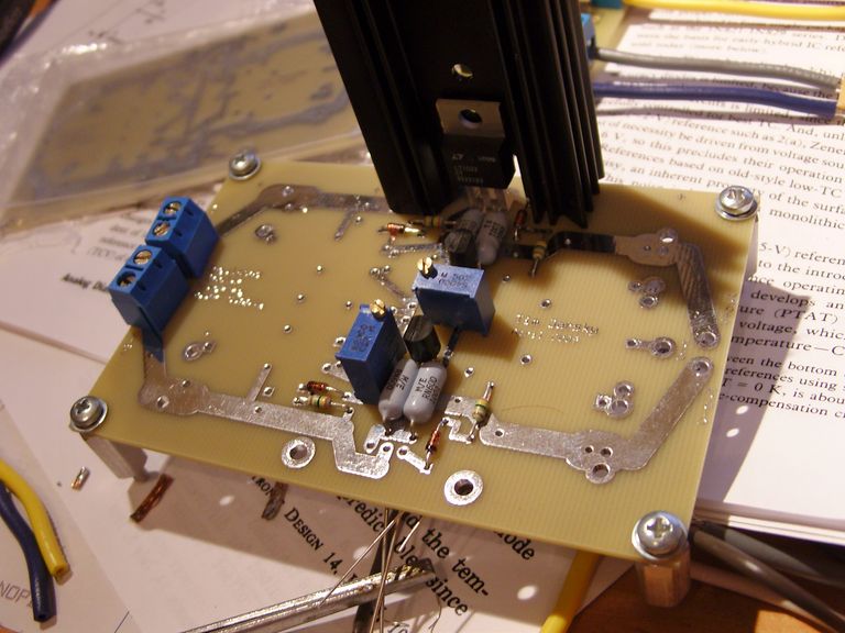
Not only the pins, but the heatsinks themselves look like they will touch some tracks. The anodizing on most heatsinks is thin, and should not be relied on for electrical insulation.marce said:Nice looking boards.
Something I didnt notice on the artworks, the heat sink pin looks close to the power track, be careful of any shorts when you assemble the PCB.
thanks for the comments.
I did notice the heatsink sitting on the power track and was a bit annoyed. Live and learn i guess. Not sure where else i could have run the power track though. I might have been able to squeeze it around the other side of the heat sink pin if i pushed everything towards the center but then my heatsinks wouldn't be as close to the edge of the board.
I will likely stick a thermal pad between the heatsink and the board unless there is a better way? Maybe a coat of paint.
The problem with a thermal pad is that it is thick enough to offset the heatsink from the regulator. I would have to raise the regulator to compensate. Since i went out of my way to keep the parts as close as possible to the regulator i find this solution unpleasant as well.
Some thin insulation, not paint. This is unfortenatley part of the fun of PCB design. General tecnique with PTH components and heatsinks, is find out what potential the heatsink pad on the device is at, it is usualy connected to a pin internaly. Then have a copper flood the size of the heatsink connected to that signal, that way you know your safe. It happens, and quite often it isn't obvious till you first assemble the board. Another way is to add the heatsink outline to your component outline, then you have an indication on the board when your laying out where the heatsink is.
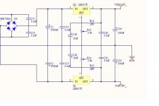
I am newbie to the power supplies . I am using the LM 3x7 series for the tda1541a DAC analog output stage. pls take a look
I wonder R11, C29, C24 suitable for the purpose of driving a simple transimpedance amplifier.
Further thots on this matter, I will try to put in charge transfer supply by ECDesigns before LM 3x7 and also put in TL431 shunt after LM3x7. What is your view ?
I wonder R11, C29, C24 suitable for the purpose of driving a simple transimpedance amplifier.
Further thots on this matter, I will try to put in charge transfer supply by ECDesigns before LM 3x7 and also put in TL431 shunt after LM3x7. What is your view ?
Attachments
ccschua said:I am newbie to the power supplies . I am using the LM 3x7 series for the tda1541a DAC analog output stage. pls take a look
I wonder R11, C29, C24 suitable for the purpose of driving a simple transimpedance amplifier.
Further thots on this matter, I will try to put in charge transfer supply by ECDesigns before LM 3x7 and also put in TL431 shunt after LM3x7. What is your view ?
I would implement the LM3x7 series as recommended in the data sheet or i would do this:
http://www.diyaudio.com/forums/showthread.php?postid=1833337#post1833337
Very interesting circuit!In the data sheet for the LT1033 negative adjustable regulator there is a typical application schematic for a tracking regulator that i am interested in but don't understand. I like the simplicity of the design as all the tracking regulators i am familiar with use opamps.
here is the schematic from the data sheet
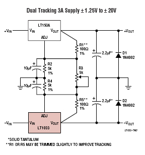
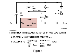
here is the more common implementation as well as the formula for calculating resistor values to set the output voltage.
my two questions are:
1. how do you adapt the formula to calculate resitor values for the tracking regulator?
2. how does the circuit match a voltage change at the output of one regulator in the other regulator?
I simulated it, and i think that it works like this:
Ir1 and Ir5 are always going to be 12mA, because of the 1.2v across that resistors. That's all the available current, and it's going down thru the resistor network.
R3 is connected to the top of R2 and the bottom of R5, so whatever r3 you use, Vr3 = Vr2+Vr4 = 2*Vr2 = 2*Vr4.
That means, that with r3=r2=r4, Ir3 is going to be 2*Ir2.
Ir1=Ir2+Ir3=Ir2+2*Ir2=Ir2*(1+2)=Ir2*3
So, in this case, Ir2 = Ir1/3, while in a standard circuit, all the current from R1 flows thru R2. This has the effect of dividing R2 by 3.
Then, by reducing R3 further, more current goes there, instead of thru R2 and R4, reducing the voltage drop there, and thus, the output voltage.
- Status
- This old topic is closed. If you want to reopen this topic, contact a moderator using the "Report Post" button.
- Home
- Amplifiers
- Power Supplies
- LT Dual Tracking 3A Regulated Power Supply 1.25V to 20V